Large-area seed for ammonothermal growth of bulk gallium nitride and method of manufacture

a gallium nitride and ammonothermal growth technology, applied in the field of crystalline materials, can solve the problems of high defect densities of epitaxial films, inability to grow these materials on a suitable gan substrate, and inability to provide low cost, so as to achieve high quality and cost-effective

Active Publication Date: 2010-03-25
SLT TECH
View PDF4 Cites 87 Cited by
  • Summary
  • Abstract
  • Description
  • Claims
  • Application Information

AI Technical Summary

Benefits of technology

[0012]One or more benefits may be achieved using one or more of the specific embodiments. As an example, the present device and method provides a substantially flat and large area seed crystal having high quality suitable for an ammonothermal or like process of crystal growth. In a specific em

Problems solved by technology

Although some of these products are available in the commercial market today, lack of a suitable GaN substrate on which to grow these materials remains a limitation to both performance and providing low cost, volume production of devices.
Heteroepitaxial approaches to growth of (Al,In)GaN containing compounds result in epitaxial films with high defect densities due to the large lattice mismatch, chemical dissimilarity and thermal expansion coefficient difference between the

Method used


Image

  • Large-area seed for ammonothermal growth of bulk gallium nitride and method of manufacture
  • Large-area seed for ammonothermal growth of bulk gallium nitride and method of manufacture
  • Large-area seed for ammonothermal growth of bulk gallium nitride and method of manufacture

Examples


example 1

[0057]In a specific embodiment, the substrate is c-plane-oriented sapphire, of any miscut orientation angle (i.e. within 10 degrees of (0001)). Both sides of the wafer are polished, for example with chemical-mechanical polishing, to provide atomically smooth surfaces suitable for epitaxy. In this embodiment molecular beam epitaxy (MBE) is the growth technique utilized to produce the nitride containing epitaxial layers. In this embodiment, one side of the wafer is first coated with a metal such as Ti or Pt, a refractory metal such as W, Mo, Ta, a silicide or nitride of one of these metals, among others, or any combination of these, in order to facilitate heat transfer to the substrate during MBE growth. The thickness of the metal containing layers could range in thickness from 0.5 to 2 microns but is not limited to this range. The metal containing layers can be deposited for example by e-beam evaporation, sputtering, chemical vapor deposition or a combination of these or other deposi...

example 2

[0063]In another embodiment the substrate is c-plane-oriented sapphire, of any miscut orientation angle (i.e. within 10 degrees of (0001)). Both sides of the wafer are polished, for example with chemical-mechanical polishing, to provide atomically smooth surfaces suitable for epitaxy. In this embodiment metal organic chemical vapor deposition (MOCVD) is the growth technique utilized to produce the nitride containing epitaxial layers. In this embodiment the substrate could be cleaned with organic solvents such as, but not limited to, acetone, methanol and isopropanol, with or without use of an ultrasonic bath. The sample should be spin-dried or blown dry with nitrogen and introduced into the MOCVD growth chamber. Preparation for growth could include pre-baking and annealing in H2, for example >1000° C. Metalorganic sources such as trimethylgallium (TMGa), triethylgallium (TEGa), trimethylaluminum (TMAl), or trimethlyindium (TMIn2) with H2 or N2 carrier gas may be used with NH3 as pre...

example 3

Preparation of a Seed Crystal

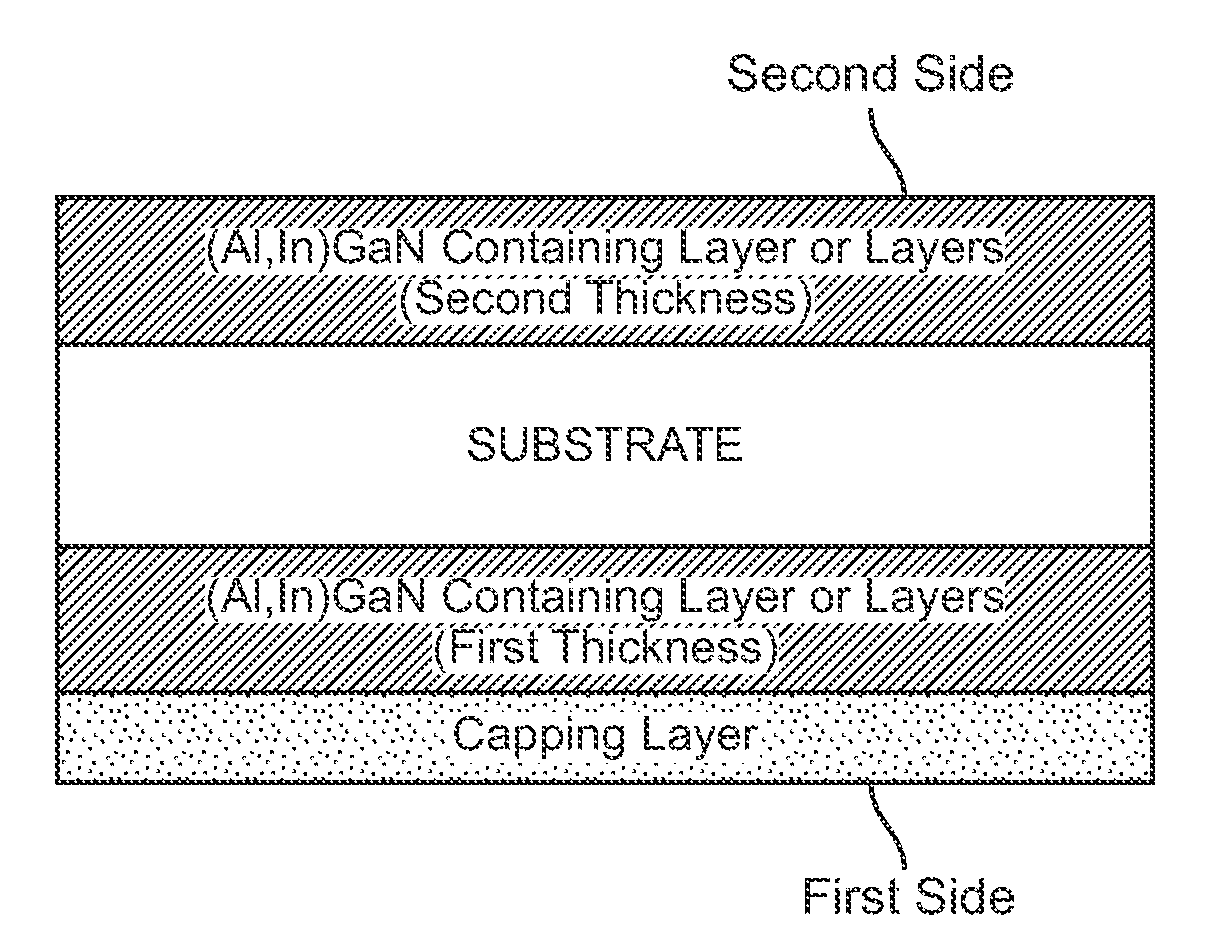
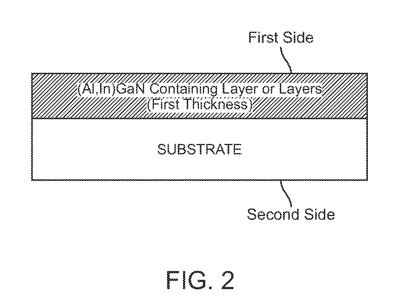
[0065]An approximately 4 μm thick GaN layer is epitaxially grown by metalorganic chemical vapor deposition (MOCVD) on one side of a 2 inch, c-plane, double-side polished sapphire wafer. The wafer is then flipped over and placed back in an MOCVD reactor. An approximately 4 μm thick GaN layer is epitaxially grown on the remaining exposed sapphire surface, producing a sapphire wafer with a 4 μm thick GaN layer on each side of the sapphire wafer.

[0066]Following is an example illustrative of the present invention. It should be understood that this is presented as an example only, and should not be considered as limiting the scope of this invention which would include other embodiments not shown. Of course, there are other variations, modifications, and alternatives.

Example 4

Preparation of a Seed Crystal

[0067]An approximately 4 μm thick GaN layer is epitaxially grown by MOCVD on one side of a 2 inch, c-plane, double-side polished sapphire wafer. The GaN layer ...


PUM

PropertyMeasurementUnit
Lengthaaaaaaaaaa
Lengthaaaaaaaaaa
Thicknessaaaaaaaaaa

Abstract

A high-quality, large-area seed crystal for ammonothermal GaN growth and method for fabricating. The seed crystal comprises double-side GaN growth on a large-area substrate. The seed crystal is of relatively low defect density and has flat surfaces free of bowing. The seed crystal is useful for producing large-volume, high-quality bulk GaN crystals by ammonothermal growth methods for eventual wafering into large-area GaN substrates for device fabrication.

Description

CROSS-REFERENCES TO RELATED APPLICATIONS[0001]This application claims priority to U.S. Provisional Application No. 61 / 096304 (Attorney Docket No 027364-003600US) filed Sep. 11, 2008 and U.S. Provisional Application No. 61 / 178460 (Attorney Docket No. 027364-006400US) filed May 14, 2009, commonly assigned, both of which are incorporate by reference in their entirety herein. This application is related to U.S. Patent Application of Attorney Docket No. 027364-005310US, filed Sep. 9, 2009, commonly assign, and of which is incorporate by reference in its entirety herein.STATEMENT AS TO RIGHTS TO INVENTIONS MADE UNDER FEDERALLY SPONSORED RESEARCH AND DEVELOPMENT[0002]NOT APPLICABLEREFERENCE TO A “SEQUENCE LISTING,” A TABLE, OR A COMPUTER PROGRAM LISTING APPENDIX SUBMITTED ON A COMPACT DISK[0003]NOT APPLICABLEBACKGROUND OF THE INVENTION[0004]The present invention relates generally to crystalline materials. More particularly, the present invention provides a seed crystal and method using bac...

Claims


Application Information

Patent Timeline
IPC IPC(8): C30B23/02B31B1/60B32B9/00
CPCC30B7/105C30B23/02C30B25/02C30B29/403C30B29/406H01L21/0237Y10T156/10H01L21/02609H01L21/0262H01L21/02631H01L21/02642H01L21/02647H01L21/0254
Inventor POBLENZ, CHRISTIANESPECK, JAMES S.
Owner SLT TECH
Why Eureka
Try Eureka