

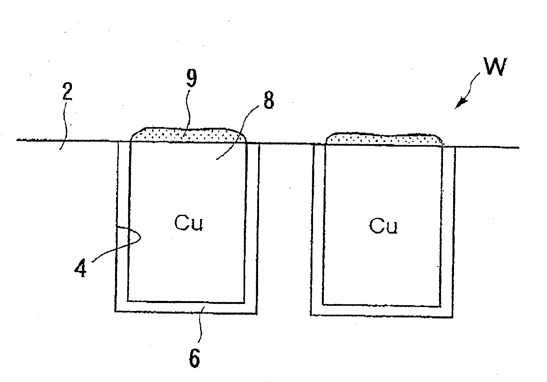
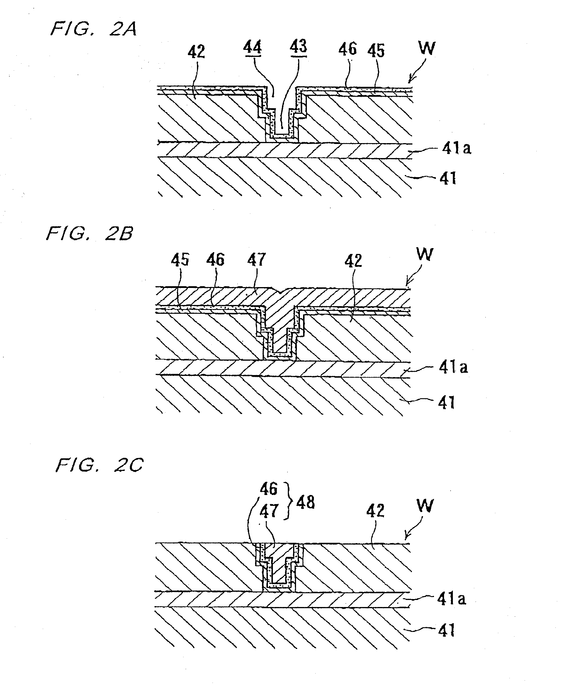
Semiconductor device and method for manufacturing the same, and processing liquid
a technology of conductive film and semiconductor device, which is applied in the direction of semiconductor/solid-state device details, liquid/solution decomposition chemical coating, coating, etc., can solve the problems of adversely affecting the intended resistance reduction, and achieve the effect of uniform thickness and less dependence on interconnect pattern
- Summary
- Abstract
- Description
- Claims
- Application Information
AI Technical Summary
Benefits of technology
Problems solved by technology
Method used
Image

Examples
example 1
[0094]A 200 mm wafer, in which an isolated interconnect 62 of copper having a length of about 3 mm and a width of 0.25 μm, linearly connecting pads 60, 60, as shown in FIG. 5A, and a dense interconnect 66 of copper, having a length of about 300 mm and a width of 0.25 μm, arranged parallel with a spacing of 0.25 μm and connecting pads 64, 64, as shown in FIG. 5B, are co-present, was prepared as a test sample. The interconnects 62, 66 were formed by forming a barrier layer of Ta and a copper seed layer by sputtering over the wafer surface with interconnect recesses formed therein, and then filling copper into the recesses by electroplating, followed by CMP to flatten the surface.
[0095]First, the sample was cut, and the cut sample was immersed in oxalic acid (2 wt %) at room temperature for one minute, followed by cleaning with pure water. The sample was then subjected to catalyst treatment by immersing it in a mixed solution of 0.1 g / L PdCl2 and 0.1 M HCl for 30 seconds, followed by c...
example 2
[0097]The same sample as in Example 1 was prepared, and an alloy film (interconnect protective film) was formed on the interconnects in the same manner as in Example 1, except for using a plating solution (processing solution) having the below-described composition. The thickness and the composition of the alloy film were determined in the above-described manner.
Composition of plating solution (mol / L)CoSO4•7H2O0.05K3C6H5O7•H2O0.3H3BO30.55K2WO40.002H3PO2 (aqueous solution)0.2pH9.0
[0098]As a result, the thickness t1 of the alloy film 68 formed on the surface of the isolated interconnect 62, shown in FIG. 6A, was found to be 100 nm, while the thickness t2 of the alloy film 70 formed on the surface of the dense interconnect 66, shown in FIG. 6B, was found to be 20 nm. The film thickness ratio t1:t2 is 5:1 (t1:t2=5:1), which ratio indicates an improvement over conventional ones (e.g., about 6.5:1). The composition Co:W:P (atomic %) of the alloy film was found to be 88:2:10 (Co:W:P (atomi...
PUM
| Property | Measurement | Unit |
|---|---|---|
| pH | aaaaa | aaaaa |
| temperature | aaaaa | aaaaa |
| temperature | aaaaa | aaaaa |
Abstract
Description
Claims
Application Information