Semiconductor integrated circuit device and IC card using the same

a technology of integrated circuit and ic card, which is applied in the direction of data processing power supply, semiconductor/solid-state device details, instruments, etc., can solve the problems of difficult to suppress the increase in the chip area and the consumption current, the difficulty of performing a process, and the long time it takes for the chip to start the operation. , to achieve the effect of reducing the voltage loss, increasing the size of the pmos transistor, and reducing the cost of operation

Inactive Publication Date: 2010-04-08
RENESAS ELECTRONICS CORP
View PDF7 Cites 22 Cited by
  • Summary
  • Abstract
  • Description
  • Claims
  • Application Information

AI Technical Summary

Benefits of technology

[0015]Further, the power supply switch circuit disclosed in the patent document 2 has to use two PMOS transistors requiring large transistor size in order to interrupt a current path generated via a parasitic diode formed between the drain and source terminals of the PMOS transistors forming the power supply switch circuit and the substrate terminal. Consequently, to reduce a voltage loss caused by the power supply switch circuit in the case where the power supply voltage supplied from the power supply voltage terminal is low, it

Problems solved by technology

Since sufficient voltage is not supplied to the internal power supply line during the period, it becomes difficult to perform a process such as determination of an operation mode and the like, and it takes long time for a chip to start the operation.
In particular, in the case where the power suppl

Method used


Image

  • Semiconductor integrated circuit device and IC card using the same
  • Semiconductor integrated circuit device and IC card using the same
  • Semiconductor integrated circuit device and IC card using the same

Examples


first embodiment

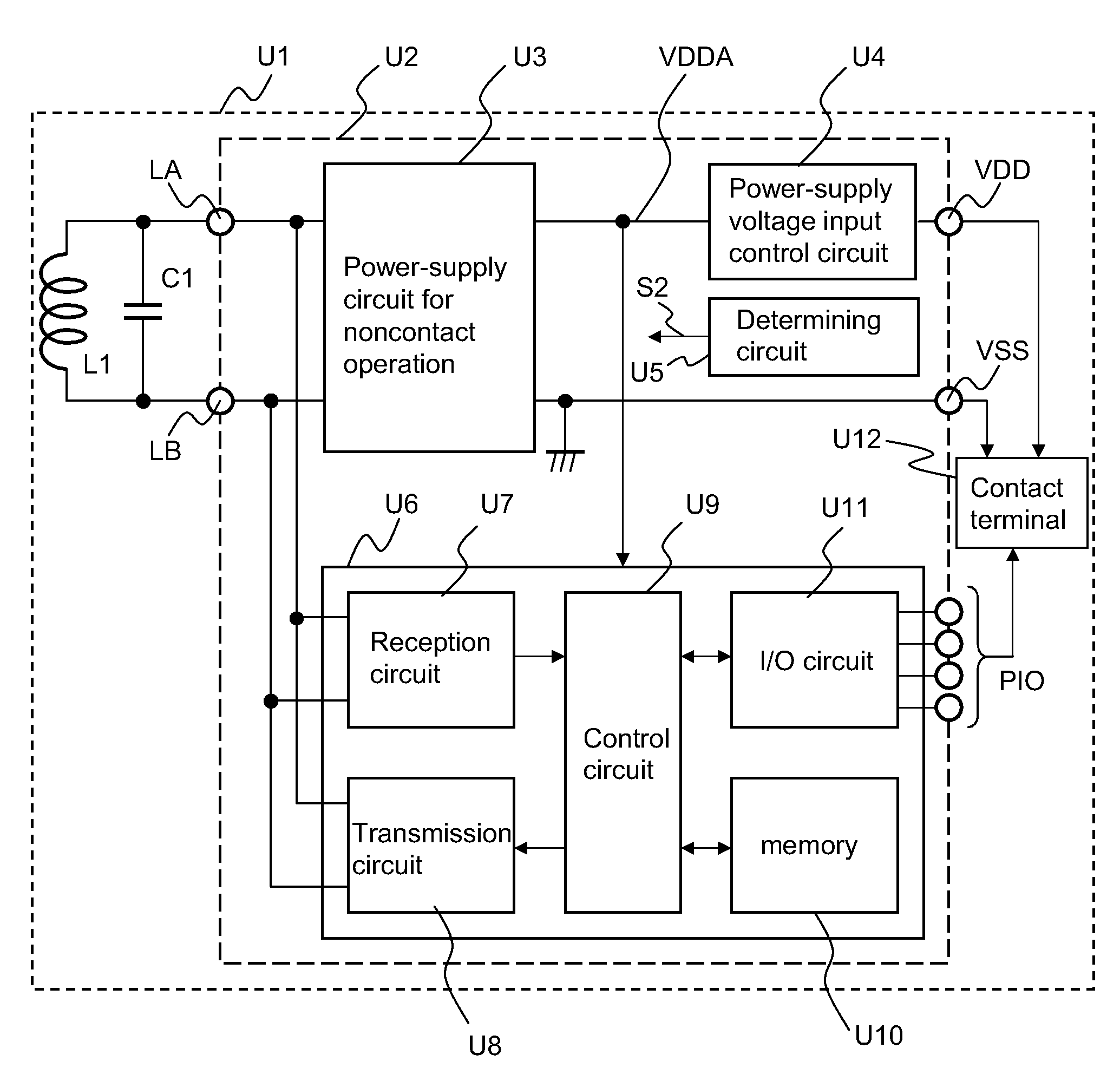
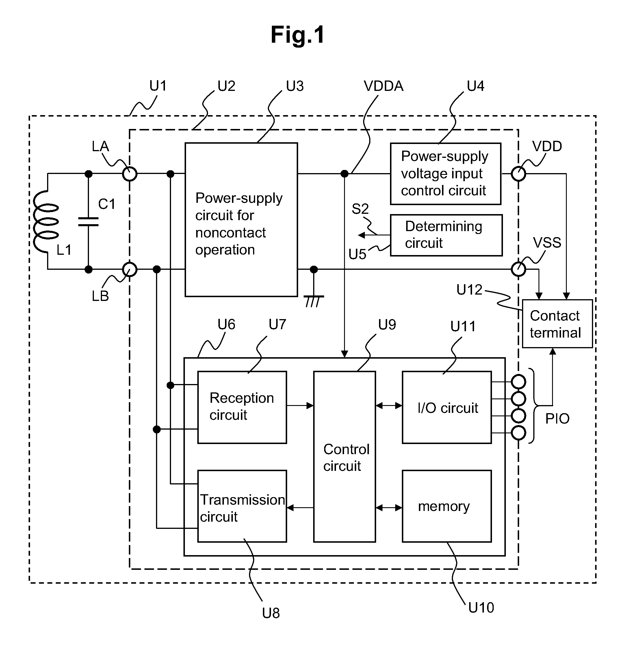
[0035]FIG. 1 is a block diagram of a basic configuration illustrating a first embodiment of a semiconductor integrated circuit device and an IC card of the present invention.

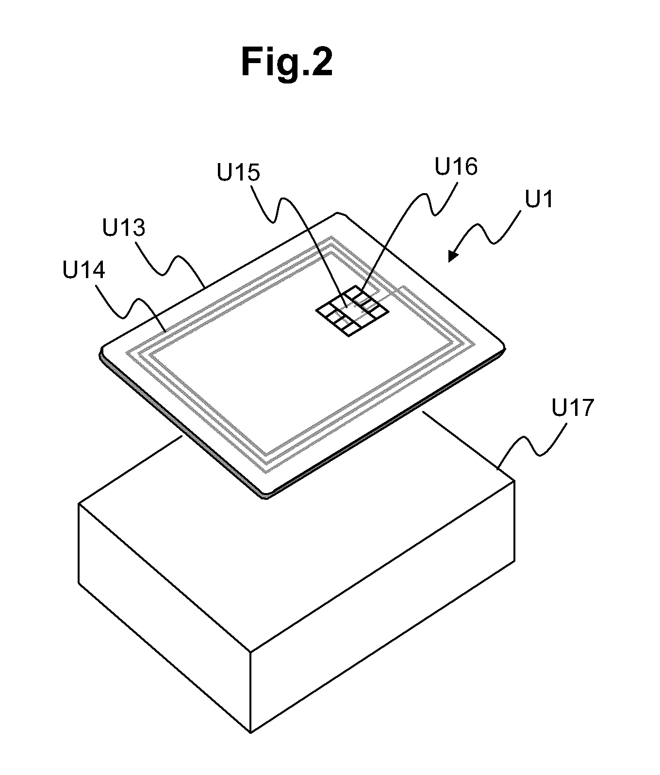
[0036]In FIG. 1, U1 denotes an IC card, U2 denotes a semiconductor integrated circuit device mounted on the IC card U1, and L1 indicates an antenna mounted on the IC card U1. A capacitor CA coupled to the antenna L1 in parallel is a component of a resonant circuit. The resonant capacitor CA is adjusted also in consideration of a parasitic capacitor and the like, so that it is not always coupled. The semiconductor integrated circuit U2 has a power supply circuit U3 for noncontact operation, a power-supply voltage terminal input control circuit U4, a contact / noncontact determining circuit U5, and an internal circuit U6 and also has antenna terminals LA and LB for coupling the antenna L1, a power-supply voltage terminal VDD, a ground terminal VSS, and signal input / output terminals PIO coupled to an external contact...

second embodiment

[0091]FIG. 8 is a basic configuration diagram showing another configuration of the power-supply voltage input control circuit U4 mounted on the semiconductor integrated circuit device of a second embodiment. To make explanation of the invention clear, the noncontact power-supply circuit U3 and the contact / noncontact determining circuit U5 mounted on the semiconductor integrated circuit device U2, and the power-supply voltage terminal VDD and the ground terminal VSS configuring the contact terminal U12 are shown.

[0092]In FIG. 8, the PMOS transistor M1 is coupled between the power-supply voltage terminal VDD and the internal power-supply line VDDA. To the substrate voltage of the PMOS transistor M1, the voltage line VDDH to which output voltage of the substrate potential control circuit B1 is supplied is coupled. To the gate terminal of the PMOS transistor M1, the control signal S1 generated by the voltage control circuit B2 and the pull-up circuit B3 is input. To the power-supply vol...

third embodiment

[0113]FIG. 9 is a basic configuration diagram showing another configuration of the power-supply voltage input control circuit U4 mounted on the semiconductor integrated circuit device of a third embodiment. To make explanation of the invention clear, the noncontact power-supply circuit U3 and the contact / noncontact determining circuit U5 mounted on the semiconductor integrated circuit device U2, and the power-supply voltage terminal VDD and the ground terminal VSS configuring the contact terminal U12 are shown.

[0114]In FIG. 9, the PMOS transistor M1 is coupled between the power-supply voltage terminal VDD and the internal power-supply line VDDA. To the substrate voltage of the PMOS transistor M1, the voltage line VDDH to which output voltage of the substrate potential control circuit B1 is supplied is coupled. To the gate terminal of the PMOS transistor M1, the control signal S1 generated by the voltage control circuit B2 and the pull-up circuit B3 is input.

[0115]The voltage control...


PUM


Abstract

The present invention enables a power-supply voltage terminal and an internal circuit to be isolated from each other in a noncontact operation without largely increasing a chip area in a semiconductor integrated circuit device for an IC card. A semiconductor integrated circuit device comprises: a first power supply circuit for rectifying and smoothing an AC signal supplied from an antenna to an antenna terminal, thereby obtaining a DC voltage in a first power-supply line; a second power supply circuit comprising a voltage control circuit for controlling gate terminal voltage of a first MOS transistor disposed between a power supply terminal to which power is input from the outside and the first power supply line; a substrate potential control circuit for forming source voltage of the first MOS transistor as a substrate voltage; and a second MOS transistor which makes substrate voltage and gate voltage of the first MOS transistor conductive in the case of using the voltage generated by the first power supply circuit as a power supply, and which makes the substrate voltage and the gate voltage nonconductive in the case of using a power supply from an external terminal.

Description

CLAIM OF PRIORITY[0001]The present application claims priority from Japanese patent application JP 2008-256948 filed on Oct. 2, 2008, the content of which is hereby incorporated by reference into this application.FIELD OF THE INVENTION[0002]The present invention relates to a power supply control technique suitably applied to a semiconductor integrated circuit device or the like mounted on an IC card and, more particularly, to a semiconductor integrated circuit device selectively operated on a power supply voltage generated from an electromagnetic wave received by an antenna provided for an IC card or a power supply voltage supplied from the outside via a contact terminal provided for the IC card, and to an IC card using the semiconductor integrated circuit.BACKGROUND OF THE INVENTION[0003]A contact-type IC card internally having a semiconductor integrated circuit having the functions of a CPU, a memory, and the like and having, on the surface of the card, a contact terminal with the...

Claims


Application Information

Patent Timeline
IPC IPC(8): G06F1/28G06K19/077G06K19/07
CPCG06K19/0701G06K19/07769G06K19/0723
Inventor WATANABE, KAZUKIYONEA, NOBUAKI
Owner RENESAS ELECTRONICS CORP
Why Eureka
Try Eureka