Method for Depositing Conformal Amorphous Carbon Film by Plasma-Enhanced Chemical Vapor Deposition (PECVD)

a technology of conformal amorphous carbon and chemical vapor deposition, which is applied in the direction of chemical vapor deposition coating, coating, metallic material coating process, etc., can solve the problems of low-k dielectric material devices with little or no surface defects or feature deformation problems, and increase the likelihood of defects on the substrate surfa

Active Publication Date: 2010-04-15
APPLIED MATERIALS INC
View PDF7 Cites 429 Cited by
  • Summary
  • Abstract
  • Description
  • Claims
  • Application Information

AI Technical Summary

Benefits of technology

[0014]In another embodiment, a method is provided for processing a substrate including positioning a substrate in a substrate processing chamber, introducing a hydrocarbon source having a carbon to hydrogen atom ratio greater than 1:2 into the processing chamber, introducing a plasma initiating gas selected from the group consisting of hydrogen, helium, argon, nitrogen, and combinations thereof into the processing chamber, with the hydrocarbon source having a volumetric flow rate to plasma initiating gas volumetric flow rate ratio of 1:2 or greater, wherein the hydrocarbon source and the plasma initiating gas are introduced into the processing chamber by a gas distributor position between 400 mils and 600 mils from the substrate surface, generating a plasma in the processing chamber at a RF power of 1 W / cm2 or less and a temperature between about 0° C. to about 100° C., and forming a conformal amorphous carbon layer on the substrate.

Problems solved by technology

Integrated circuits have evolved into complex devices that can include millions of transistors, capacitors and resistors on a single chip.
Producing devices having low-k dielectric materials with little or no surface defects or feature deformation is problematic.
Low-k dielectric materials having a dielectric constant less than about 3.0 are often porous and susceptible to being scratched or damaged during subsequent process steps, thus increasing the likelihood of defects being formed on the substrate surface.
Such low-k dielectric materials are often brittle and may deform under conventional polishing processes, such as chemical mechanical polishing (CMP).
As device sizes shrink and pattern structure becomes more complex and difficult to manufacture, an etch hardmask is becoming more important as available photoresists are failing to meet the etching resistance requirements and photoresists are simply being used for image transfer rather than as an etch mask in a lithography and etching process.
Additionally as feature sizes are reduced, photoresists materials have trouble correctly transferring patterns due to the limitation of light wavelengths and pattern sizes.
The lack of complete coverage of sidewalls 114 by non-conformal amorphous carbon layer 112 may also lead to photoresist poisoning of the material under non-conformal carbon layer 112, which is known to damage electronic devices.

Method used


Image

  • Method for Depositing Conformal Amorphous Carbon Film by Plasma-Enhanced Chemical Vapor Deposition (PECVD)
  • Method for Depositing Conformal Amorphous Carbon Film by Plasma-Enhanced Chemical Vapor Deposition (PECVD)
  • Method for Depositing Conformal Amorphous Carbon Film by Plasma-Enhanced Chemical Vapor Deposition (PECVD)

Examples


Embodiment Construction

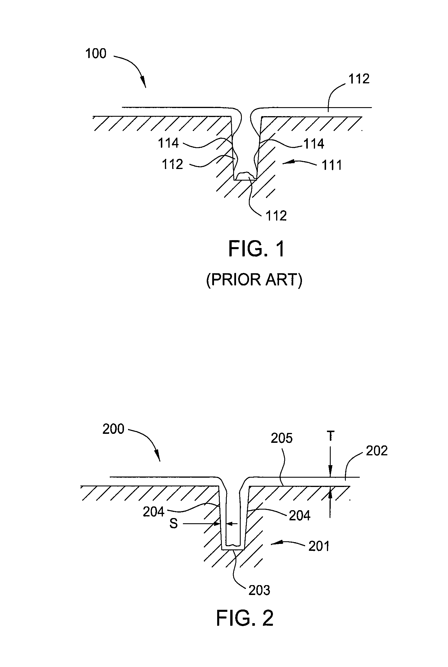
[0024]Embodiments described herein generally provide methods for depositing amorphous carbon materials (a-C:H) with improved conformality in a chemical vapor deposition system. Conformality of a layer is typically quantified by a ratio (which may be represented as a percentage) of the average thickness of a layer deposited on the sidewalls of a feature to the average thickness of the same deposited layer on the field, or upper surface, of the substrate. Layers deposited by the methods described herein are observed to have a conformality of greater than about 30%, such as 70% or greater, about 7:10 or grater, such as about 80% or greater, about 4:5 greater, to about 100%, about 1:1. For example, the prior art non-conformal amorphous carbon layer 112 as shown in FIG. 1 would be considered to have 0% conformity due to the lack of a layer deposition on the sidewalls 114.

[0025]In particular, methods are provided for improved conformal deposition of an a-C:H layer. Conformal deposition ma...


PUM


Abstract

Methods and apparatus for depositing an amorphous carbon layer on a substrate are provided. In one embodiment, a deposition process includes positioning a substrate in a substrate processing chamber, introducing a hydrocarbon source having a carbon to hydrogen atom ratio of greater than 1:2 into the processing chamber, introducing a plasma initiating gas selected from the group consisting of hydrogen, helium, argon, nitrogen, and combinations thereof into the processing chamber, with the hydrocarbon source having a volumetric flow rate to plasma initiating gas volumetric flow rate ratio of 1:2 or greater, generating a plasma in the processing chamber, and forming a conformal amorphous carbon layer on the substrate.

Description

CROSS-REFERENCE TO RELATED APPLICATIONS[0001]This application claims benefit of U.S. provisional patent application Ser. No. 61 / 105,348, filed Oct. 14, 2008, which is herein incorporated by reference.BACKGROUND OF THE INVENTION[0002]1. Field of the Invention[0003]Embodiments of the present invention generally relate to the fabrication of integrated circuits and particularly to the deposition of an amorphous carbon layer on a semiconductor substrate.[0004]2. Description of the Related Art[0005]Integrated circuits have evolved into complex devices that can include millions of transistors, capacitors and resistors on a single chip. The evolution of chip design continually requires faster circuitry and greater circuit density. The demand for faster circuits with greater circuit densities imposes corresponding demands on the materials used to fabricate such integrated circuits. In particular, as the dimensions of integrated circuit components are reduced to sub-micron dimensions, it has ...

Claims


Application Information

Patent Timeline
Patent Type & Authority Applications(United States)
IPC IPC(8): H01L21/312
CPCC23C16/26C23C16/45523H01L21/3146H01L21/3141C23C16/5096H01L21/02274H01L21/02115H01L21/02205H01L21/0228H01L21/02592
Inventor LEE, KWANGDUK DOUGLASMORII, TAKASHISUZUKI, YOICHIRATHI, SUDHASEAMONS, MARTIN JAYPADHI, DEENESHKIM, BOK HOENPAGDANGANAN, CYNTHIA
Owner APPLIED MATERIALS INC
Why Eureka
Try Eureka