Ingap heterojunction barrier solar cells

a solar cell and heterojunction technology, applied in the field of ingap heterojunction barrier solar cells, can solve the problems of diodes with higher dark currents than structures employing thin wells, low conversion efficiency, and low efficiency of incident solar power, so as to increase the short-circuit current, maximize the photocurrent, and enhance the photovoltaic conversion efficiency of hbsc

Active Publication Date: 2010-04-22
KOPIN CORPORATION
View PDF5 Cites 49 Cited by
  • Summary
  • Abstract
  • Description
  • Claims
  • Application Information

AI Technical Summary

Benefits of technology

[0013]Employing an ultrawide layer of narrow band-gap material enhances the photovoltaic conversion efficiency of the HBSC with respect to that of traditional semiconductor solar cells. Because HBSCs use ultrawide wells instead of multiple thin layers, HBSCs are in some ways the opposite of traditional quantum-well or quantum-dot solar cells: the wide band-gap material of the PN junction offers a potential increase in the open-circuit voltage, whereas the narrow band-gap material in quantum-well and quantum-dot solar cells enables a potential increase in the short-circuit current. In addition, the electric field and barrier profiles of an HBSC can be tailored to maximize the photocurrent at forward bias and to enhance thermionic emission of photogenerated carriers. Thus, HBSCs offer significant increases in open-circuit voltage without compromising the short-circuit current of ei

Problems solved by technology

In traditional single-junction semiconductor solar cells, the conversion efficiency is typically limited to less than 25% of the incident solar power.
At higher bias, however, the insertion of GaAs wells leads to a marked degradation in the dark current.
In addition

Method used


Image

  • Ingap heterojunction barrier solar cells
  • Ingap heterojunction barrier solar cells
  • Ingap heterojunction barrier solar cells

Examples


example 1

InGaP Absorber Structure

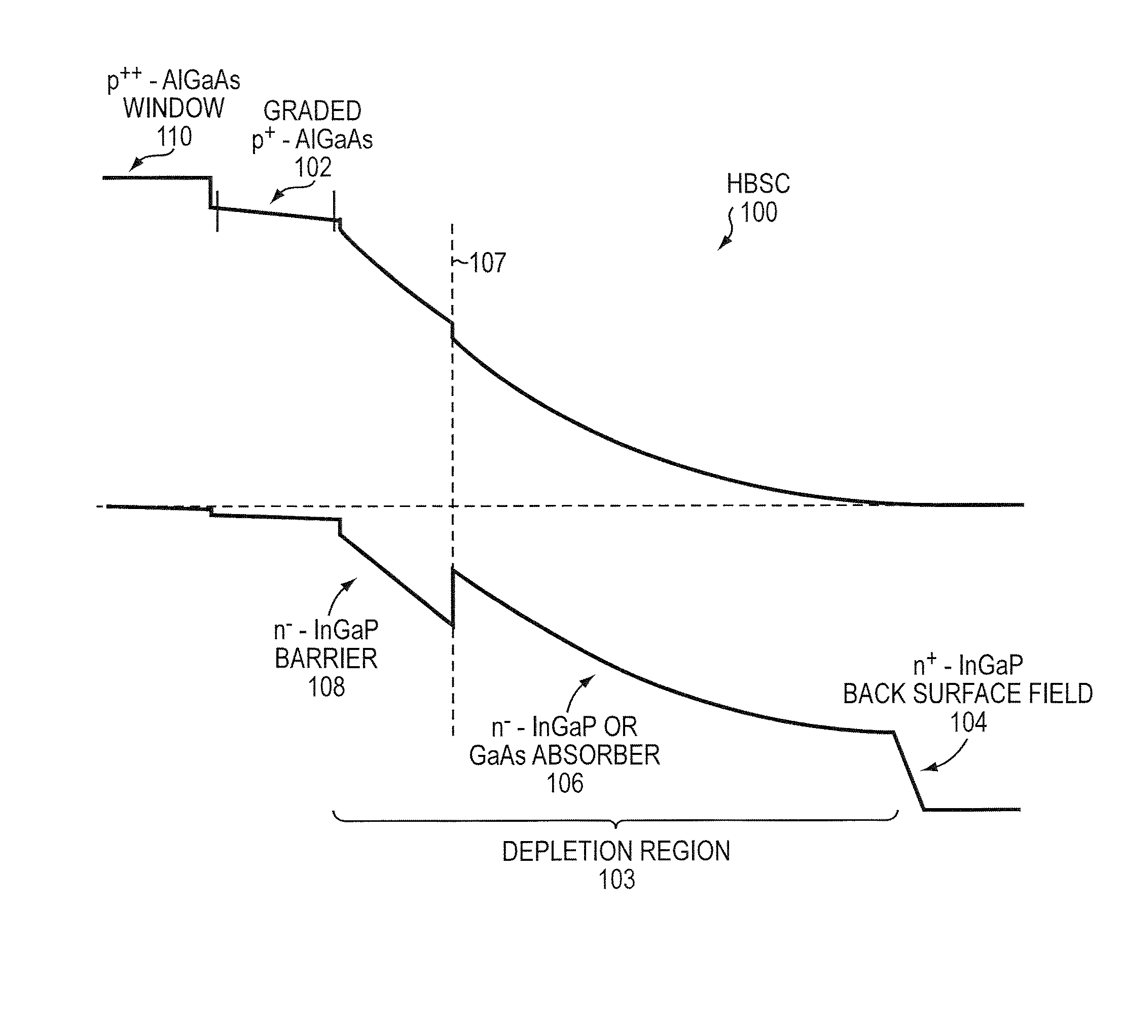
[0036]HBSCs employing InGaP alloys for both the barrier and absorber layers werebuilt by inserting 30-50 nm wide, lattice-mismatched, gallium-rich InGaP layers into nearly lattice-matched, but slightly indium-rich InGaP-based PIN diode controls. The example HBSC structures were grown on MOCVD tools also employed for Kopin's high-volume heterojunction bipolar transistor (HBT) wafer production. The InGaP alloys are largely disordered, with an energy gap of 1.895 eV when perfectly matched to GaAs, as characterized by photoluminescence and X-ray diffraction measurements. The devices were fabricated with Kopin's standard Quick Lot process used to characterize HBT material. Further details on HBT production can be found in co-assigned U.S. Pat. No. 7,566,948, incorporated herein by reference in its entirety.

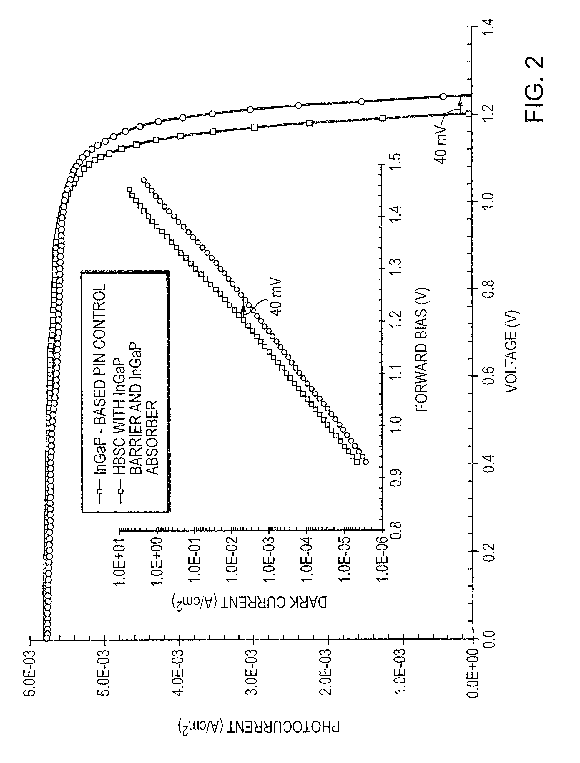
[0037]FIG. 2 is plot of measured photocurrent versus open-circuit voltage for an HBSC (circles) and a conventional InGaP-based PIN diode control (squares) illum...

example 2

GaAs Absorber Structure

[0040]In the second example, HBSCs were constructed by replacing the InGaP absorber layer with GaAs, which has a much lower energy-gap (Eg≈1.42 eV), and varying the thickness of the InGaP barrier layer using the techniques described above with respect to Example 1. [% Please provide more information on how you made these devices.]

[0041]FIG. 3 is a plot of the measured variation in dark diode current density at two bias levels of 0.8 V (squares) and 1.2 V (circles) of InGaP-based PIN diodes incorporating a wide GaAs well as a function of InGaP barrier layer thickness. The inset of FIG. 3 shows the full dark diode current versus voltage for different InGaP barrier thicknesses. Remarkably, the dark current does not begin to increase significantly until the InGaP barrier thickness drops below 50 nm, as shown in FIG. 3. Even a 30 nm thick InGaP barrier is sufficient to minimize dark current degradation at the higher bias relevant to solar cell operation.

[0042]In re...


PUM


Abstract

A new solar cell structure called a heterojunction barrier solar cell is described. As with previously reported quantum-well and quantum-dot solar cell structures, a layer of narrow band-gap material, such as GaAs or indium-rich InGaP, is inserted into the depletion region of a wide band-gap PN junction. Rather than being thin, however, the layer of narrow band-gap material is about 400-430 nm wide and forms a single, ultrawide well in the depletion region. Thin (e.g., 20-50 nm), wide band-gap InGaP barrier layers in the depletion region reduce the diode dark current. Engineering the electric field and barrier profile of the absorber layer, barrier layer, and p-type layer of the PN junction maximizes photogenerated carrier escape. This new twist on nanostructured solar cell design allows the separate optimization of current and voltage to maximize conversion efficiency.

Description

RELATED APPLICATION[0001]This application claims the benefit of U.S. Provisional Application No. 61 / 196,532, filed on Oct. 17, 2008. The entire teachings of the above application are incorporated herein by reference.GOVERNMENT SUPPORT[0002]The invention was supported, in whole or in part, by grant NNX08CB49P from the Small Business Innovative Research (SBIR) Program of the U.S. National Aeronautics and Space Administration (NASA). The Government has certain rights in the invention.BACKGROUND OF THE INVENTION[0003]The performance of photovoltaic solar arrays and the underlying solar cell devices is typically characterized by the solar electric conversion efficiency. The solar electric conversion efficiency is governed, in turn, by the amount of current induced by incident light and the operating voltage of the device. In traditional single-junction semiconductor solar cells, the conversion efficiency is typically limited to less than 25% of the incident solar power. Photons with ener...

Claims


Application Information

Patent Timeline
IPC IPC(8): H01L31/00H01L31/0232
CPCH01L31/03042H01L31/0336H01L31/065H01L31/035236Y10S977/755Y10S977/774H01L31/035209Y02E10/544
Inventor WELSER, ROGER E.
Owner KOPIN CORPORATION
Why Eureka
Try Eureka