Non-random array anisotropic conductive film (ACF) and manufacturing processes

a manufacturing process and anisotropic conductive film technology, applied in the field of anisotropic conductive film structure and manufacturing methods, can solve the problems of several major technical difficulties and limitations, and the current technology of anisotropic conductive films (acf) or z-axis conductive adhesive films (zaf) for interconnection, and achieve the effect of reducing manufacturing costs and improving resolution

Active Publication Date: 2010-04-29
POLAROID IP BV
View PDF32 Cites 85 Cited by
  • Summary
  • Abstract
  • Description
  • Claims
  • Application Information

AI Technical Summary

Benefits of technology

[0034]Briefly, in a preferred embodiment, the present invention provides a fine pitch ACF comprising a non-random array of conductive particles or filled microcavities of predetermined size, shape with partition areas to keep the particles or microcavities well separated from each other. The ACFs prepared according to the present invention also provide a better resolution, reliability of electrical connection at a lower manufacturing cost.

Problems solved by technology

Current technologies for manufacturing anisotropic conductive films (ACF) or Z-axis conductive adhesive film (ZAF) for interconnecting array of electrodes such as those in liquid crystal display interconnections, chip-on-glass, chip-on-film, flip chip bonding and flexible circuits applications, are still challenged by several major technical difficulties and limitations.
For those of ordinary skills in the art, there are still no technical solutions to overcome these difficulties and limitations.
The first difficulty faced by the conventional technologies is related to the slow and costly processes commonly employed in the preparation and purification of the narrowly dispersed conductive particles commonly implemented as the anisotropic conductive medium.
The second difficulty is related to the preparation of ACF for high resolution or fine pitch application.
However, the increase in the particle concentration may also result in an increase in the conductivity in the x-y direction due to the probability of increase of undesirable particle-particle interaction or aggregation.
However, the concentration of the conductive particles that may be used in the processes is still limited by the statistic probability of particle-particle contact or aggregation.
The resultant filled dimples or perforation is relatively rigid and not easy to deform during bonding.
Moreover, the filling process often results in an under-filled dimple or perforation due to the presence of solvent or diluent in the paste or ink.
A high electrical resistance in the bonding area and a poor environmental and physicomechanical stability of the electric connections are often the issues of this type of ACFs.
The metal beading process is very susceptible to the presence of impurity or contamination on the surface / interface.
The size of the metal bead may be formed by this process is also relatively limited.
A spike on the bead surface is quite difficult to form.
Moreover, the metal bead is not easy to deform during bonding and results in a high electrical resistance in the bonding area more often with a poor environmental and physicomechanical stability of the electric connections.
In either the direct or direct printing of conductive particles on a substrate, the size of the printed dots tends to be relatively big and non-uniform and missing particles or aggregation of particles are problems for reliable connections.
The resultant ACF is not suitable for fine pitch applications.
However, the mechanical integrity, conductivity, and compressibility of metallic columns are still potential problems for reliable connections.
The manufacturing of ACF involves an expensive and tedious process including the steps of photolithographic exposure of resist on a metal substrate, development of photoresist, electroforming, stripping of resist, and finally overcoating of an adhesive.
However, the resultant high cost ACF is not very suitable for practical applications partly because the compressibility or the ability to form conformation contacts with the electrodes and corrosion resistance of the electroformed metallic (Ni) columns are not acceptable and result in a poor electrical contact with the device to be connected to.
The inability to form conformation contacts with electrodes remains to be an issue.
It results in high electrical resistance in the bonding area and a poor long term stability of the electrical connection.
Moreover, it's very difficult to form a spike on the top of the electroformed metal columns.
The processes of using ferromagnetic particles and the subsequent removal of them are costly and the pitch size of the resultant ACF is also limited by the loading of the ferromagnetic particles and conductive particles.
As a result, the effectiveness of the spikes in penetrating into the oxide surface is quite low.

Method used


Image

  • Non-random array anisotropic conductive film (ACF) and manufacturing processes
  • Non-random array anisotropic conductive film (ACF) and manufacturing processes
  • Non-random array anisotropic conductive film (ACF) and manufacturing processes

Examples


examples

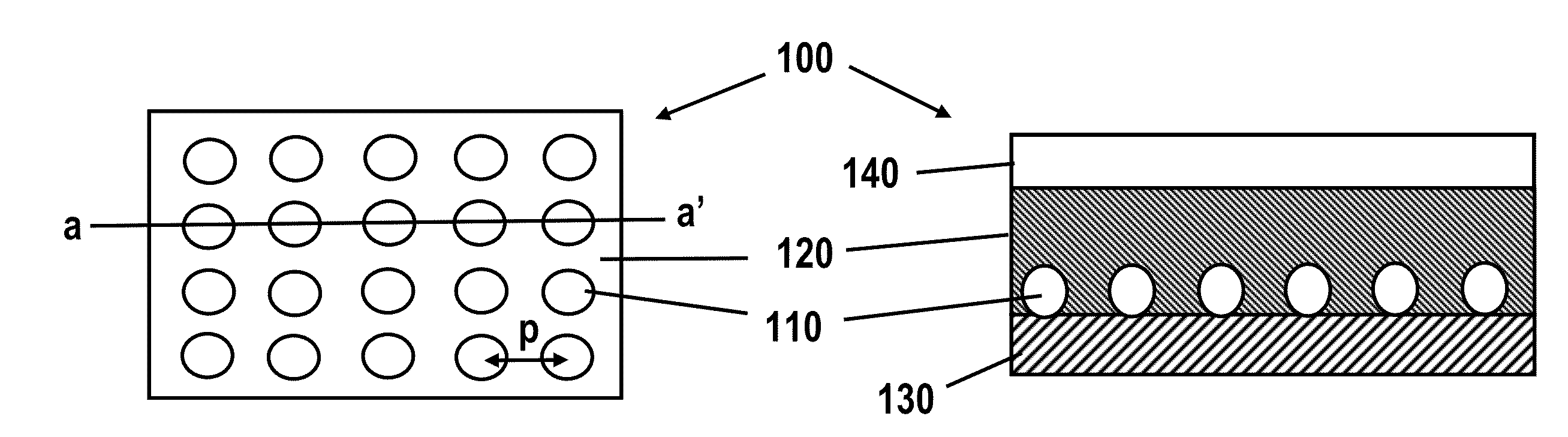
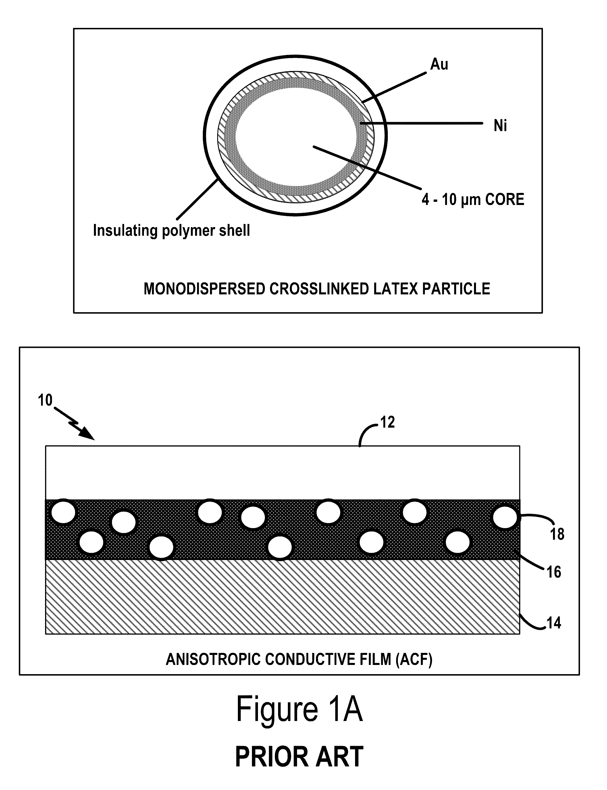
[0141]The following examples are given to enable those skilled in the art to understand the present invention more clearly and to practice it. They should not be construed as the limits of the present invention, but should be considered as illustrative and representative examples. For the demonstration of the particle filling and transfer, two types of commercially available conductive particles (110) were used: the Ni / Au particles from Nippon Chemical through its distributor, JCI USA, in New York, a subsidiary of Nippon Chemical Industrial Co., Ltd., White Plains, N.Y. and the Ni particles from Inco Special Products, Wyckoff, N.J.

[0142]Generation of Microcavity Array Pattern on Polyimide Film by Laser Ablation

[0143]Two types of microcavity arrays were produced on letter size 8.5″×11″, approximately 3-mil heat stabilized polyimide film (PI, 300 VN from Du Pont.) The targeted dimension of the microcavities was about 6 um (diameter)×about 2.0 um (partition)×about 4 um (depth) and abou...


PUM

PropertyMeasurementUnit
vibration frequencyaaaaaaaaaa
peeling angleaaaaaaaaaa
surface temperatureaaaaaaaaaa

Abstract

Structures and manufacturing processes of an ACF array using a non-random array of microcavities of predetermined configuration, shape and dimension. The manufacturing process includes fluidic filling of conductive particles onto a substrate or carrier web comprising a predetermined array of microcavities, or selective metallization of the array followed by filling the array with a filler material and a second selective metallization on the filled microcavity array. The thus prepared filled conductive microcavity array is then over-coated or laminated with an adhesive film. Cavities in the array, and particles filling the cavities, can have a unimodal, bimodal, or multimodal distribution.

Description

[0001]This application is a Continuation-in-Part Application of, and claims the benefit of, co-pending non-provisional U.S. patent application Ser. No. 11 / 418,414, filed on May 3, 2006, both of which applications being assigned to the same assignee hereof; this Application also claims the benefit of U.S. Provisional Patent Application No. 60 / 690,406, which has a priority filing date of Jun. 13, 2005; and this Application hereby incorporates by reference in their respective entirety, the aforementioned non-provisional Patent Application and provisional Patent Application.BACKGROUND OF THE INVENTION[0002]1. Field of the Invention[0003]This invention relates generally to the structures and manufacturing methods of an anisotropic conductive film (ACF). More particularly, this invention relates to new structures and manufacturing processes of an ACF of improved resolution and reliability of electrical connection at a significantly lower production cost.[0004]2. Description of the Related...

Claims


Application Information

Patent Timeline
Patent Type & Authority Applications(United States)
IPC IPC(8): B32B38/00B32B37/00B32B38/04
CPCB32B27/16Y10T428/24289B32B27/36H01B1/22H05K3/323H05K2201/10378H05K2203/0113H05K2203/0338B32B3/30B32B7/06B32B7/12B32B27/08H01L23/48H05K1/0296H05K3/00H01L24/29H01L2224/16225H01L2224/32225H01L2224/73204H01L2924/07811B32B27/34H01L2924/00B32B27/28B32B27/30B32B27/32B32B27/38B32B27/40B32B3/08B32B2264/02B32B2264/10B32B2307/202B32B2307/706B32B2457/00B32B2457/08B32B2457/202H01L2924/12042H01L2224/95101
Inventor LIANG, RONG-CHANGCHUNG, JERRYTSENG, CHINJENROKUTANDA, SHUJISUN, YUHAOCHUANG, HSIAO-KEN
Owner POLAROID IP BV
Why Eureka
Try Eureka