

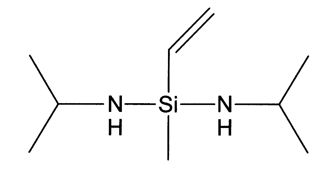
Amino Vinylsilane Precursors for Stressed SiN Films
a technology of amino vinylsilane and precursors, applied in the field of integrated circuit fabrication, can solve the problems of increasing compressive stress further, and achieve the effect of enhancing chemical vapor deposition and increasing intrinsic compressive stress
- Summary
- Abstract
- Description
- Claims
- Application Information
AI Technical Summary
Benefits of technology
Problems solved by technology
Method used
Image

Examples
example
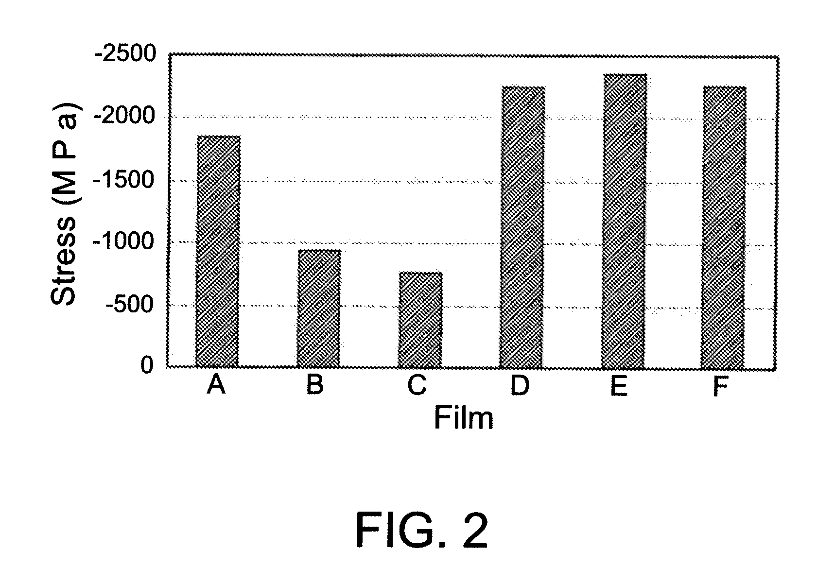
[0022]Depositions conditions for Runs A-F and the corresponding film stress obtained in Table 1, below, are as follows. Deposition temperature was 400 C. In these examples, properties were obtained from sample films that were deposited onto medium resistivity (8-12 Ωcm) single crystal silicon wafer substrates. All depositions were performed on an Applied Materials Precision 5000 system in a 200 mm DXZ chamber fitted with an Advanced Energy 2000 RF generator. The plasma is single frequency of 13.56 MHz.
[0023]In the Table 1 examples, thickness and optical properties, such as refractive index of the dielectric films, were measured on an SCI Filmtek Reflectometer. The refractive index is measured using 632 nm wavelength light. Fourier Infrared Spectroscopy (FTIR) data was collected on the wafers using a Thermo Nicolet 750 system in a nitrogen purged cell. Background spectra were collected on similar medium resistivity wafers to eliminate CO2 and water from the spectra. Data was obtained...
example 2
[0029]Under process condition A listed in Table 1, the stress of films using non-vinyl precursor (such as BTBAS) is lower than that for (BIPAVMS)
TABLE 2ThicknessDep. RateStressPrecursor(nm)(nm / min)RI(MPa)BIPAVMS20813.91.97−1849BTBAS13613.61.97−1034
example 3
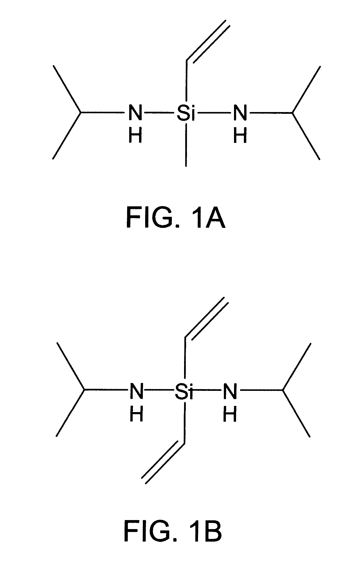
[0030]Under process condition A listed in Table 1, but an alternative tool and showerhead configuration, the stress of films deposited increases as the number of vinyl groups increases in precursor.
TABLE 3PrecursorVinyl groupsStress (MPa)BIPAVMS1−1200BIPADVS2−1705
PUM
| Property | Measurement | Unit |
|---|---|---|
| Temperature | aaaaa | aaaaa |
| Mass flow rate | aaaaa | aaaaa |
| Mass flow rate | aaaaa | aaaaa |
Abstract
Description
Claims
Application Information