Optical microscope and spectrum measuring method
a spectrum measurement and optical microscope technology, applied in the field of optical microscope and spectrum measurement method, can solve the problems of slow reading speed, difficult uniform light application, and dark peripheral area, and achieve the effect of shortening the measurement time and reducing the number of times of measuring a spectrum
- Summary
- Abstract
- Description
- Claims
- Application Information
AI Technical Summary
Benefits of technology
Problems solved by technology
Method used
Image
Examples
first embodiment
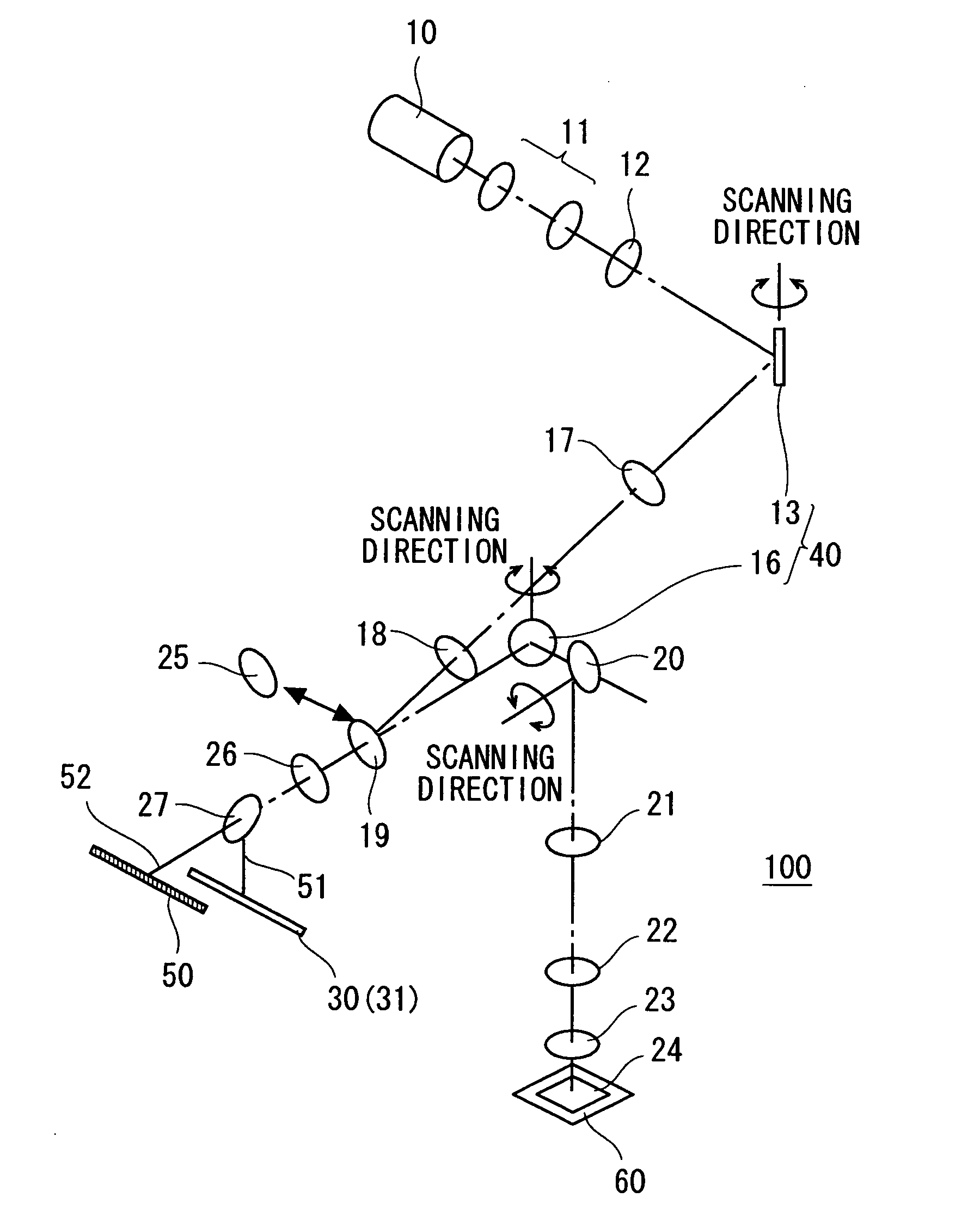
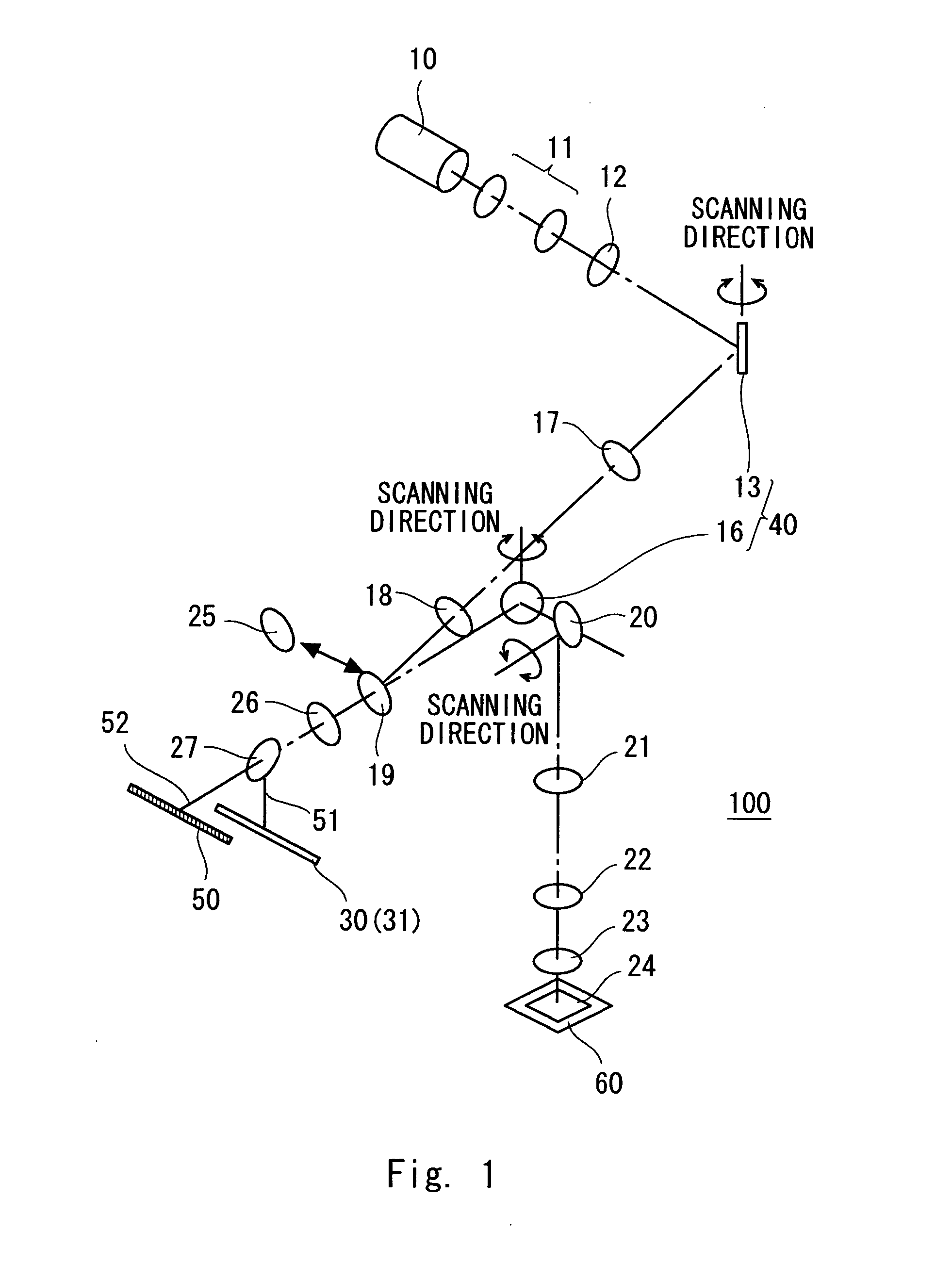
[0037]An optical microscope according to a first embodiment of the present invention is described hereinafter with reference to FIG. 1. FIG. 1 is a view schematically showing the structure of an optical system of an optical microscope 100 according to the embodiment. The optical microscope 100 includes a laser light source 10, a beam expander 11, a laser line filter 12, a Y-directional scanning unit 40, a relay lens 17, a relay lens 18, an edge filter 19, an X-directional scanning unit 20, a relay lens 21, a tube lens 22, an objective lens 23, a half mirror 25, a focusing lens 26, a switching mirror 27, a spectroscope 31, a line CCD camera 50 and a stage 60, as a structure for observing a sample 24.
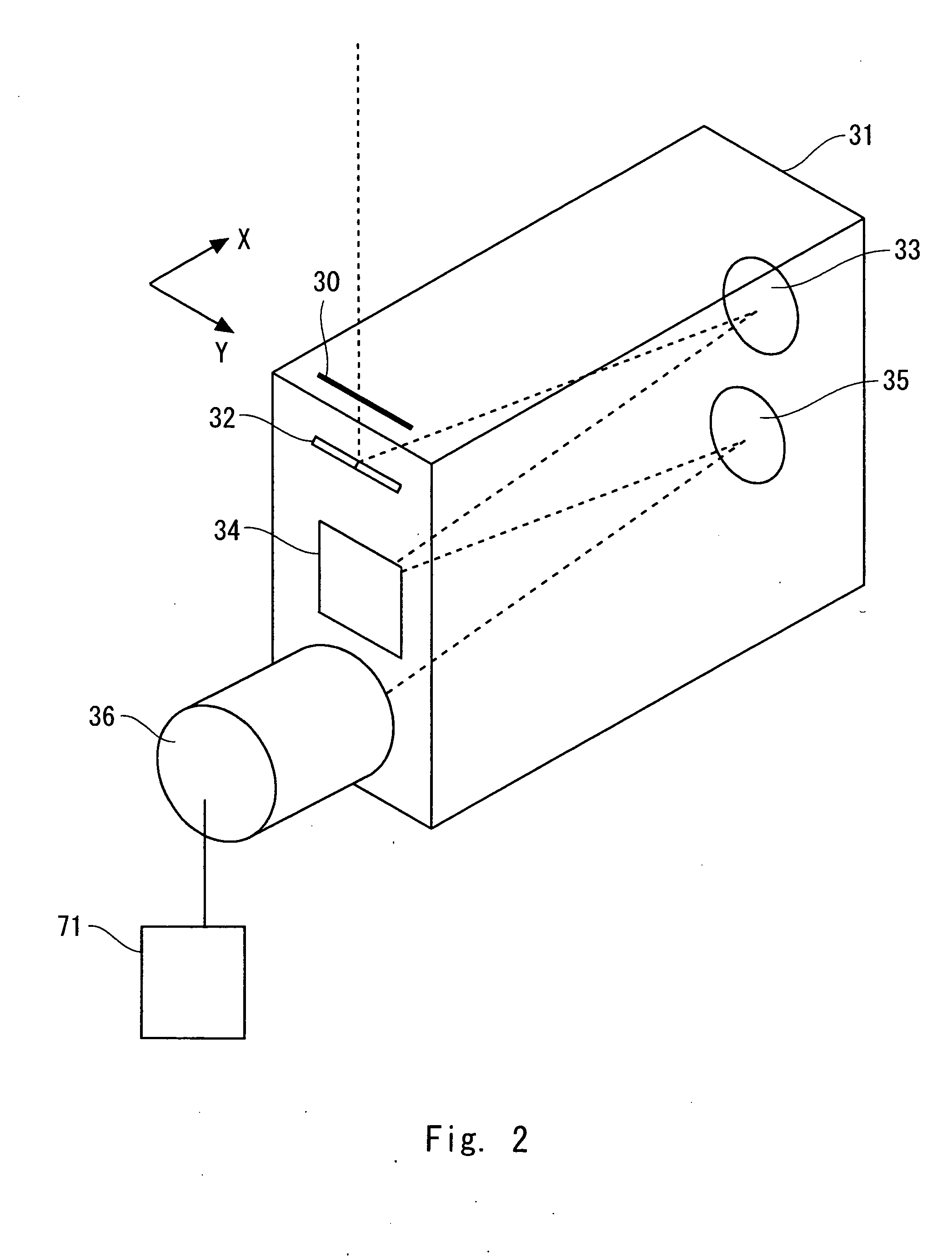
[0038]The optical microscope 100 is a Raman microscope. The optical microscope 100 allows a light beam from the laser light source 10 to enter the sample 24 and detects Raman scattered light from the sample 24 with the spectroscope 31. The spectroscope 31 disperses the Raman scattered lig...
second embodiment
[0098]An optical microscope 100 according to a second embodiment of the present invention is described hereinafter with reference to FIG. 8. FIG. 8 is a view showing an optical system of the optical microscope 100 according to the embodiment. In this embodiment, a beam splitter 56 is placed between the high-speed scanner 13 and the laser line filter 12. Light separated by the beam splitter 56 enters an automatic focus (AF) mechanism 53. The other elements are the same as those described in the first embodiment, and redundant explanation thereof is omitted. In this structure, similar advantages to the first embodiment can be obtained.
[0099]In this embodiment, Raman spectrum measurement is conducted while performing tracking of a sample surface by the AF mechanism 53. Automatic focusing (AF) is performed with use of the AF mechanism 53 during Raman spectrum measurement. The AF mechanism 53 includes a quadrant photodiode, a lens, a cylindrical lens or the like. The AF mechanism 53 perf...
third embodiment
[0103]In a third embodiment of the present invention, an optical system capable of conducting capture of a reflected image and measurement of a Raman spectrum simultaneously is employed. In this embodiment, the position of the line CCD camera 50 is different from that in the first embodiment. Further, a beam splitter 55 is placed between the edge filter 19 and the relay lens 18. Reflected light separated by the beam splitter 55 enters the line CCD camera 50 through a focusing lens 54. The other elements are the same as those described in the first embodiment, and redundant explanation thereof is omitted.
[0104]In this embodiment, capture of a reflected image and measurement of a Raman spectrum are conducted simultaneously. Therefore, the edge filter 19 and the switching mirror 27 are disposed on the optical path even during capture of a reflected image. Further, the beam splitter 55 that separates reflected light from laser light is disposed on the optical path. The beam splitter 55 ...
PUM
 Abstract
Description
Claims
Application Information


