Liquid crystal display device and manufacturing method thereof

a liquid crystal display device and switching mode technology, applied in semiconductor devices, instruments, optics, etc., can solve the problems of lowering the transmissivity and other aspects, insufficient driving, and reducing the aperture ratio, so as to achieve high throughput of liquid crystal display devices, reduce the variation in the characteristics of tfts, and high reliability

Active Publication Date: 2010-06-03
JAPAN DISPLAY WEST
View PDF1 Cites 16 Cited by
  • Summary
  • Abstract
  • Description
  • Claims
  • Application Information

AI Technical Summary

Benefits of technology

[0040]On the contrary, according to the method of manufacturing the liquid crystal display device of the above aspect of the invention, the peripheral circuit having the TFTs of which the channel regions are not covered with the passivation film is directly covered with the interlayer resin film. Therefore, since the TFTs of the peripheral circuit are prevented from being damaged, thus decreasing the variation in the characteristics o

Problems solved by technology

With the IPS mode liquid crystal display device, however, because the pair of electrodes are provided on the same layer in order to apply an electric field to the liquid crystals, there is the problem that the liquid crystal molecules, which are positioned above the pixel electrode, are inadequately driven, and this results in lowering of transmissivity and other aspects.
However, the FFS mode liquid crystal display devices disclosed in JP-A-2001-235763 and JP-A-2002-182230 has the problem that, because there is misalignment of the liquid crystal molecules due to a potential difference between the signal line and the pixel electrode, portions at the vicinity of the signal line constitute regions that do not contribute to the display and therefore the aperture ratio decreases.
Another problem is that there is a coupling capacitance between the signal line and the pixel electrode, which causes deterioration in display quality such as crosstalk.
Therefore, the liquid crystal display device disclosed in JP-A-2001-083540 and JP-A-2007-226175 can reliably provide improved aperture ratio but many layered structures have to be formed on one transparent substrate, so that more manufacturing processes are needed and the manufacturing costs will increase.
Therefore, in the liquid crystal display device of Prior Application, since it is difficult to prevent the channel regions of the TFTs in the peripheral circuits of the display area from being exposed to various chemical solutions until they are covered with the inter-electrode insulating film, the damage to the channel portion will increase, thus increasing the variation in the characteristics of the TFTs of the peripheral circuits and impairing the reliability thereof.
If the interlayer resin film has a thickness of less than 1.5 μm, steps are fo

Method used


Image

  • Liquid crystal display device and manufacturing method thereof
  • Liquid crystal display device and manufacturing method thereof
  • Liquid crystal display device and manufacturing method thereof

Examples


first embodiment

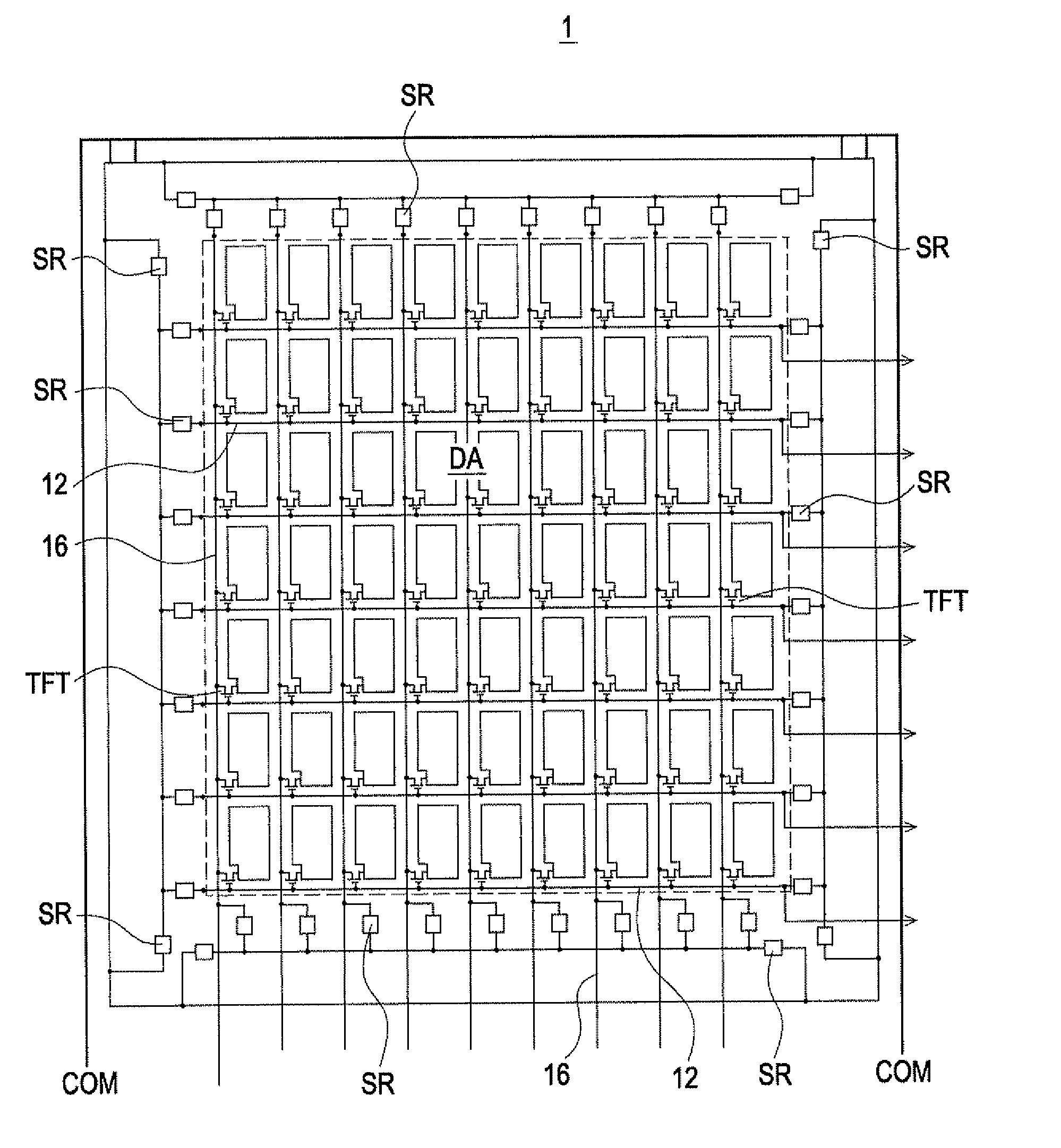
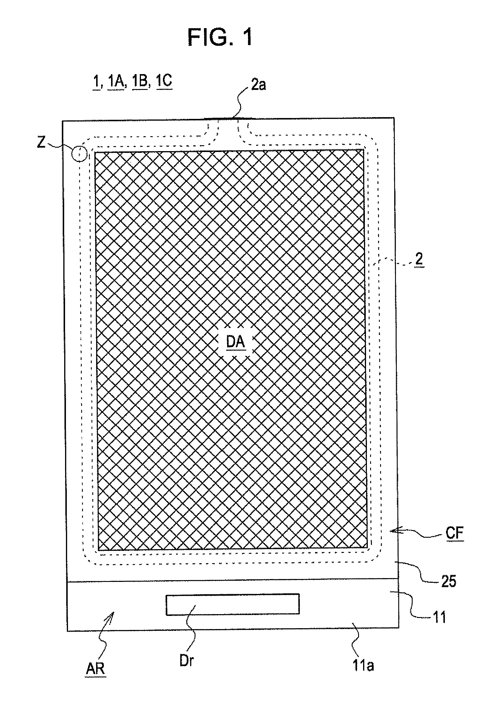
[0063]As shown in FIG. 1, a liquid crystal display device 1 according to the embodiment is a so-called chip on glass (COG) type liquid crystal display device which includes an array substrate AR, a color filter substrate CF, a sealing member 2 bonding the array substrate AR and the color filter substrate CF together, and liquid crystals 30 (see FIG. 3) enclosed in a region surrounded by the array substrate AR, the color filter substrate CF, and the sealing member 2. In this liquid crystal display device 1, a region surrounded by the sealing member 2 forms a display area DA and the peripheral portion of the display area DA serves as a frame area. The sealing member 2 has formed therein an inlet 2a for injection of the liquid crystals 30. Referring to FIG. 1, the region corresponding to the display area DA is indicated as a shaded area with a grid pattern.

[0064]The array substrate AR is configured with a transparent substrate 11 which is formed of glass or the like and has various lin...

second embodiment

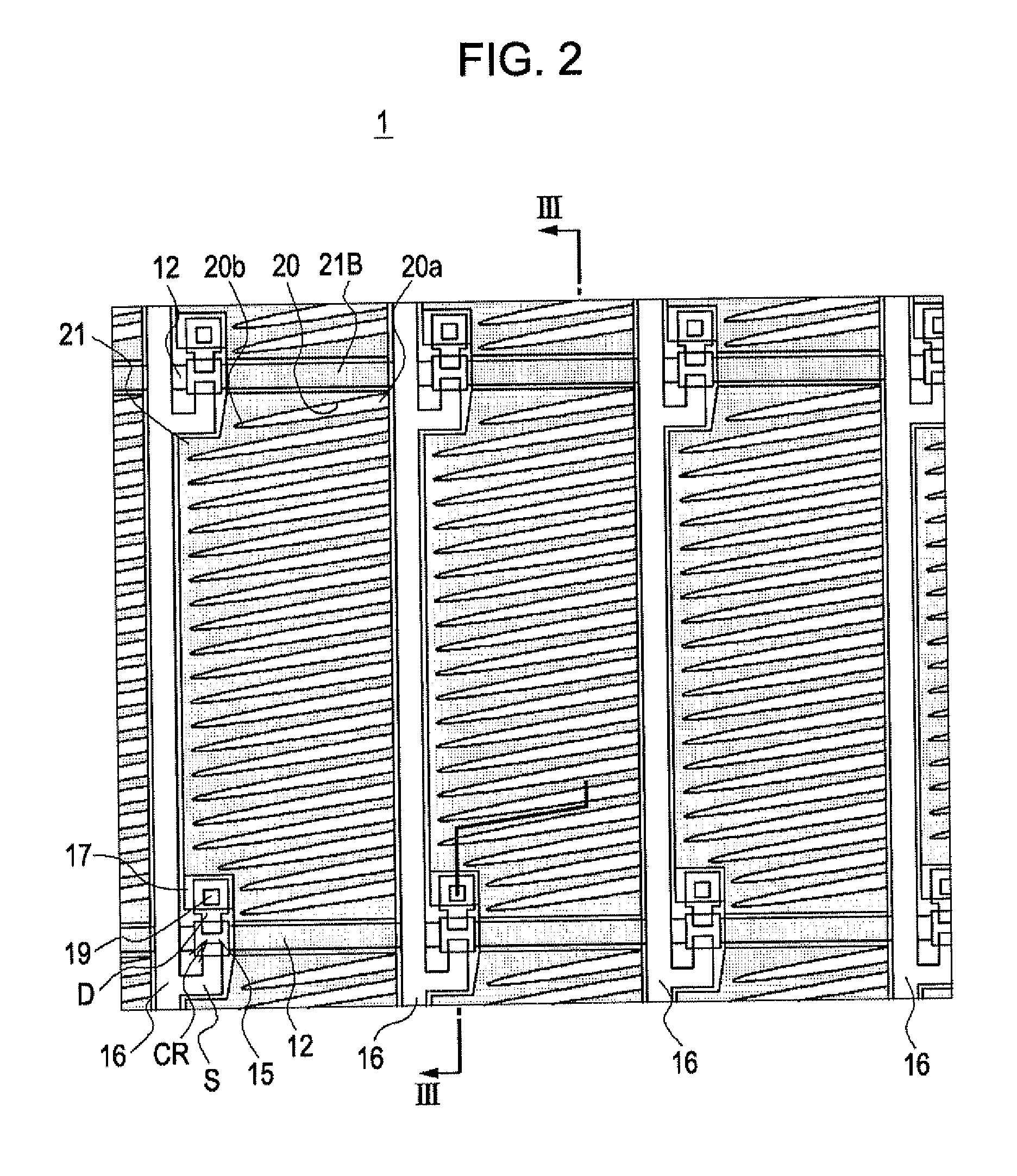
[0088]A liquid crystal display device 1A of the second embodiment has a structure such that the first electrode 17 of the display area DA extends so as to cover the TFTs used as the switching elements as viewed in plan view, as illustrated in FIGS. 8A and 9, and other structures are the same as those of the liquid crystal display device of the first embodiment.

[0089]Since the first electrode 17 is formed so as to cover the TFTs as viewed in plan view, the TFTs are covered with the first electrode 17 as well as the interlayer resin film 14 and the second insulating film 18. Therefore, according to the liquid crystal display device 1A of the second embodiment, the first electrode 17 can sufficiently function as the protective film, and it is thus possible to more effectively suppress variation in the characteristics of the switching elements due to external causes and to ensure long-term reliability of the switching elements.

third embodiment

[0090]A liquid crystal display device 1B of the third embodiment has a structure such that the second electrode 21 of the display area DA extends so as to cover the TFTs used as the switching elements as viewed in plan view, as illustrated in FIGS. 8B and 10, and other structures are the same as those of the liquid crystal display device of the first embodiment.

[0091]Since the second electrode 21 is formed so as to cover the TFTs as viewed in plan view, the TFTs are covered with the second electrode 21 as well as the interlayer resin film 14 and the second insulating film 18. Therefore, according to the liquid crystal display device 1B of the third embodiment, the second electrode 21 can sufficiently function as the protective film, and it is thus possible to more effectively suppress variation in the characteristics of the switching elements due to external causes and to ensure long-term reliability of the switching elements.


PUM


Abstract

A liquid crystal display includes an interlayer resin film covering a surface of the display area including thin film transistors, first electrodes formed of transparent conductive material on the surface of the interlayer resin film in regions defined by scan and signal lines and electrically connected to the thin film transistors. A second insulating film formed on the surface of the interlayer resin film includes the first electrodes and second electrodes formed of transparent conductive material on the second insulating film, the second electrodes having slits defined at the scan lines and signal lines. A circuit including thin film transistors with exposed channel regions is on the display area's periphery. The interlayer resin film directly covers the thin film transistors' channel regions in the display area and the peripheral area; and the surface of the display area's and peripheral circuit's interlayer resin films are covered with the second insulating film.

Description

BACKGROUND[0001]1. Technical Field[0002]The present invention relates to a fringe field switching (FFS) mode liquid crystal display device and a method for manufacturing such a device. More particularly, the invention relates to an FFS mode liquid crystal display device and a method for manufacturing such a device, in which it is not only possible to simplify the layered structures of a display area and a peripheral circuit formed on a substrate thereof, but also to decrease manufacturing costs thereof while guaranteeing moisture resistance equivalent to that of the related art, and in which a variation in the characteristics of the TFTs of the peripheral circuit is small, thus guaranteeing a highly reliable operation of such a device.[0003]2. Related Art[0004]Many of the liquid crystal display devices being used are of the vertical electric field type which has a pair of transparent substrates with electrodes and the like formed on their surfaces and a liquid crystal layer that is ...

Claims


Application Information

Patent Timeline
IPC IPC(8): G02F1/1333G02F1/13
CPCG02F1/133345G02F1/134363G02F1/136204H01L27/1248G02F2001/134372G02F2201/40G02F2001/133388G02F1/133388G02F1/134372
Inventor NAKAO, HAJIME
Owner JAPAN DISPLAY WEST
Why Eureka
Try Eureka