Semiconductor device manufacturing method and semiconductor device

a semiconductor and manufacturing method technology, applied in the direction of individual semiconductor device testing, semiconductor/solid-state device testing/measurement, instruments, etc., can solve the problems of increasing the threshold voltage due to impurity variation, reducing the total number of impurities included in the channel of the transistor, etc., to achieve the effect of reducing the threshold voltage, easy measurement, and improving the speed

Inactive Publication Date: 2010-06-10
SONY CORP
View PDF2 Cites 74 Cited by
  • Summary
  • Abstract
  • Description
  • Claims
  • Application Information

AI Technical Summary

Benefits of technology

[0029]The second semiconductor device according to the embodiment of the present invention has the opening for exposing the probing electrode connected to the transistor. Thereby the threshold voltage of the transistor can be measured easily from the opening. As a result, analytic evaluation of the transistor can be performed, and a circuit block or a transistor causing a lack of speed of a logic circuit or a lack of a voltage margin is detected. Then, the threshold voltage of the detected transistor can be corrected after completion of a wafer process or while the analytic evaluation is performed.
[0030]The first semiconductor device manufacturing method and the second semiconductor device manufacturing method according to the embodiments of the present invention can adjust the threshold voltage of...

Problems solved by technology

A problem to be solved is that as scaling advances, a total number of impurities included in the chan...

Method used


Image

  • Semiconductor device manufacturing method and semiconductor device
  • Semiconductor device manufacturing method and semiconductor device
  • Semiconductor device manufacturing method and semiconductor device

Examples


first embodiment

[First Example of Method of Manufacturing Semiconductor Device]

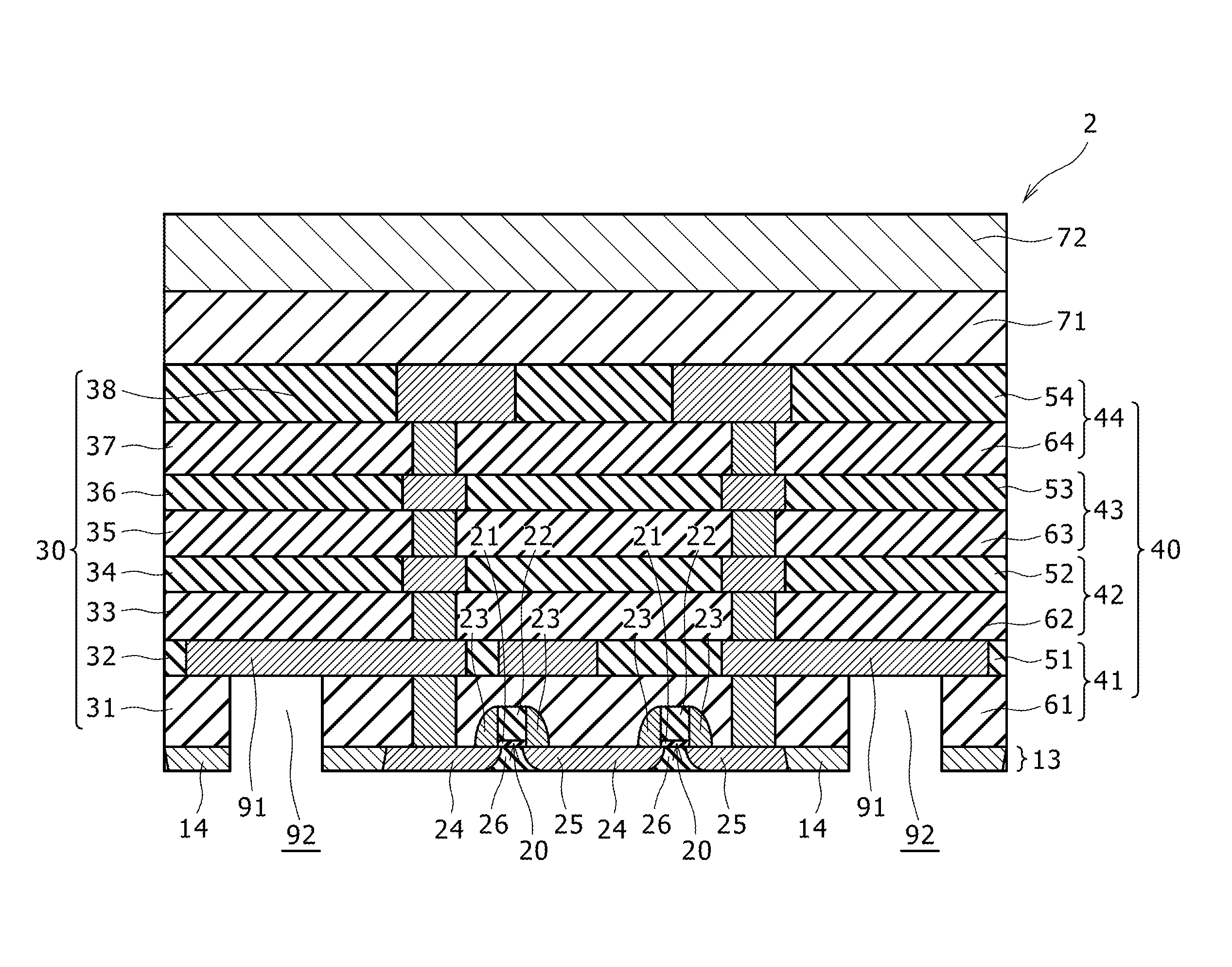
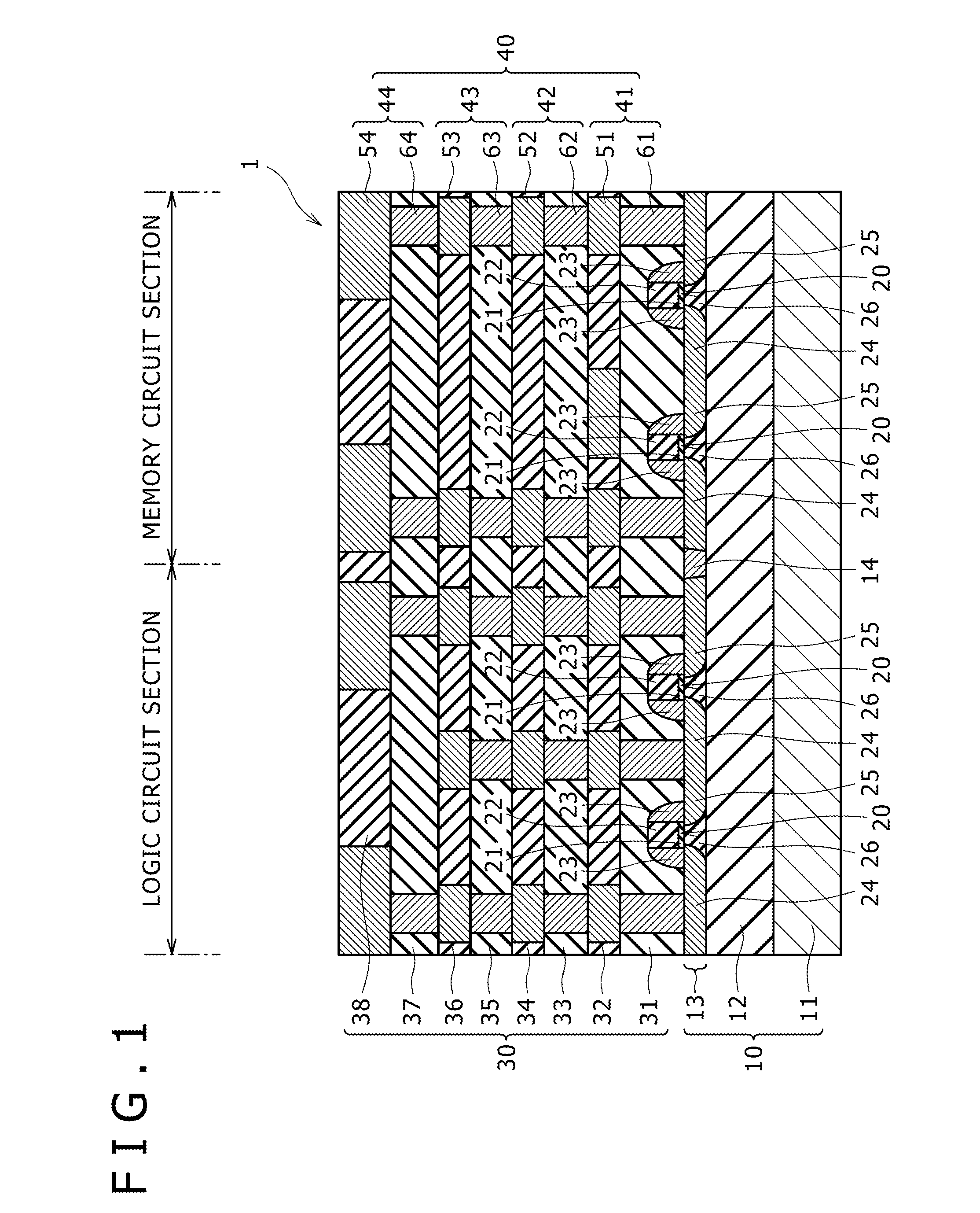
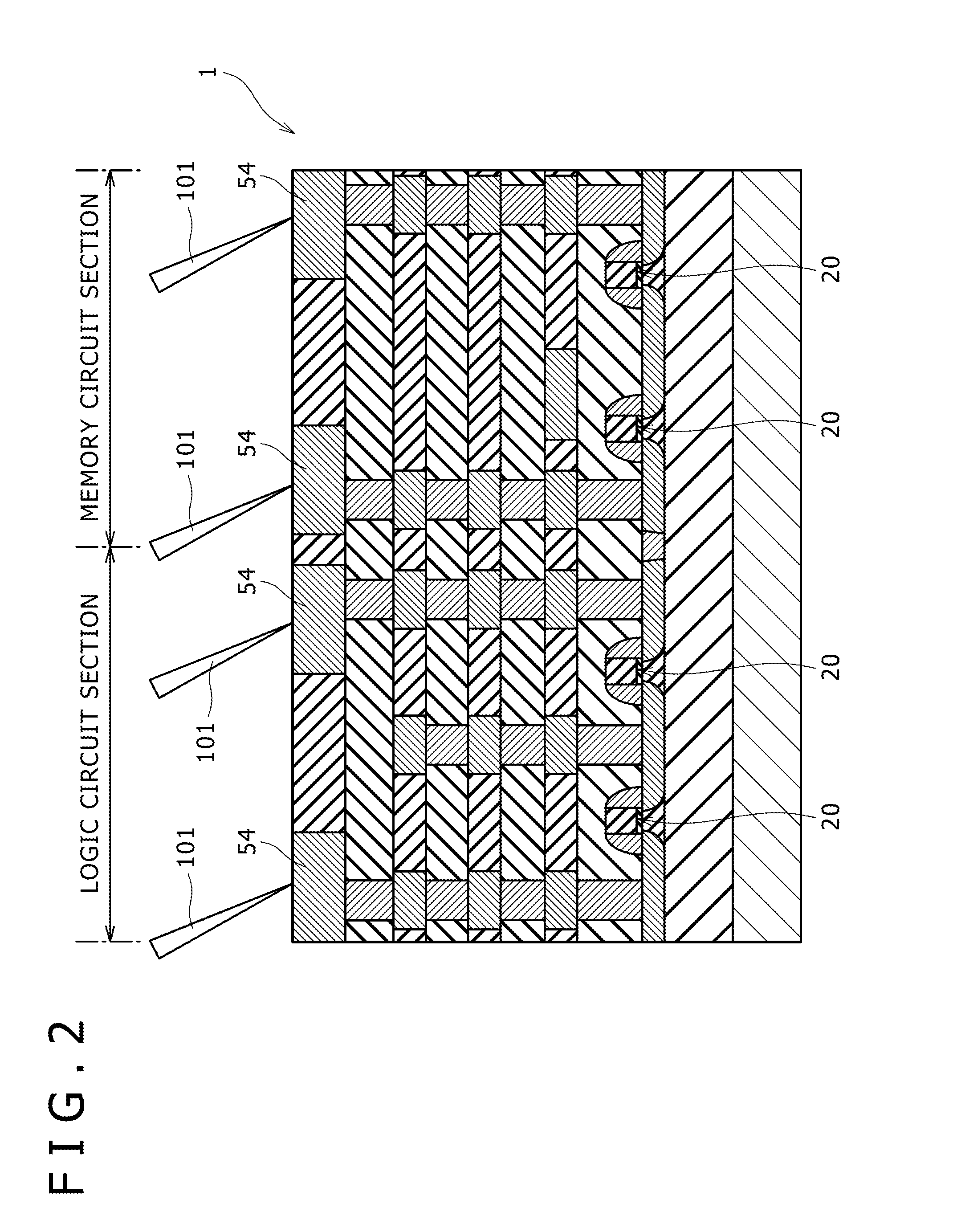
[0043]A first example of a method of manufacturing a semiconductor device according to a first embodiment of the present invention will be described with reference to manufacturing process sectional views of FIGS. 1 to 4. FIGS. 1 to 4 show N-channel transistors of a logic circuit section and an SRAM cell section as a memory circuit section as an example.

[Formation of Transistor]

[0044]As shown in FIG. 1, an SOI substrate 10 formed by laminating a substrate 11, an insulating layer 12, and a silicon layer 13 is prepared. The substrate 11 is formed by for example a silicon substrate as a semiconductor substrate having conductivity, for example. The insulating layer 12 is formed by a silicon oxide film, for example.

[0045]First, an element isolation region 14 for isolating the logic circuit section, the memory circuit section and the like from each other is formed in the silicon layer 13. The element isolation region 14 is for...

second embodiment

[Second Example of Method of Manufacturing Semiconductor Device]

[0111]A second example of a method of manufacturing a semiconductor device according to a second embodiment of the present invention will be described with reference to manufacturing process sectional views of FIGS. 5 and 6. FIGS. 5 and 6 show N-channel transistors included in a logic circuit section and a memory circuit section as an example.

[0112]As shown in FIG. 5, an SOI substrate 10 formed by laminating a substrate 11, an insulating layer 12, and a silicon layer 13 is prepared. The substrate 11 is formed by for example a silicon substrate as a semiconductor substrate having conductivity, for example. The insulating layer 12 is formed by a silicon oxide film, for example.

[0113]First, an element isolation region 14 for isolating elements from each other is formed in the silicon layer 13. The element isolation region 14 is for example formed by making a groove in the silicon layer 13 and filling in the groove with an ...

third embodiment

[First Example of Constitution of Semiconductor Device]

[0151]A first example of a semiconductor device according to the second embodiment of the present invention will be described with reference to a manufacturing process sectional view of FIG. 7.

[0152]As shown in FIG. 7, transistors 20 are formed on the surface side of a silicon layer 13 in a state of being isolated by an element isolation region 14. The element isolation region 14 is for example formed of an STI structure composed of for example a silicon oxide film, a silicon nitride film, or a silicon oxynitride film.

[0153]The transistor 20 is formed as follows.

[0154]A gate electrode 22 is formed on the surface of the silicon layer 13 with a gate insulating film 21 interposed between the gate electrode 22 and the silicon layer 13. The gate insulating film 21 is formed by a so-called high dielectric constant film of for example a hafnium oxide, a hafnium silicide oxynitride, a zirconium oxide, or a zirconium silicide oxynitride....


PUM


Abstract

A semiconductor device manufacturing method includes the steps of: forming a transistor on a surface side of a silicon layer of a silicon-on-insulator substrate, the silicon-on-insulator substrate being formed by laminating a substrate, an insulating layer, and the silicon layer; forming a first insulating film covering the transistor and a wiring section including a part electrically connected to the transistor on the silicon-on-insulator substrate; measuring a threshold voltage of the transistor through the wiring section; forming a supporting substrate on a surface of the first insulating film with a second insulating film interposed between the supporting substrate and the first insulating film; removing at least a part of the substrate and the insulating layer on a back side of the silicon-on-insulator substrate; and adjusting the threshold voltage of the transistor on a basis of the measured threshold voltage.

Description

BACKGROUND OF THE INVENTION[0001]1. Field of the Invention[0002]The present invention relates to a semiconductor device manufacturing method and a semiconductor device.[0003]2. Description of the Related Art[0004]A CPU (Central Processing Unit) and a logic device including a CPU core are composed of a logic circuit section formed mainly by various logic gates and a memory circuit section such as a shift register, a cache memory and the like. This memory circuit section is formed by an SRAM (Static Random Access Memory), for example.[0005]The performance of a logic gate or an SRAM is determined by the performance of a MOS (Metal Oxide Semiconductor) transistor forming the logic gate or the SRAM.[0006]The performance of a MOS transistor is given by the following Equation (1) expressing a drain-to-source current and Equation (2) expressing variation σVt in threshold voltage (see “Fundamentals of Modern VLSI Devices” by Taur and Ning, p. 279).Ids=β(Vgs−Vt)2 / 2  (1)σVt=q√(Na·Wdm0 / (3LW)) / C...

Claims


Application Information

Patent Timeline
IPC IPC(8): H01L29/78H01L21/66H01L23/544
CPCH01L21/84H01L22/14H01L22/20H01L27/105H01L29/78H01L27/1104H01L27/1116H01L27/1203H01L27/11H01L29/7855H10B10/18H10B10/00H10B10/12
Inventor KURODA, HIDEAKI
Owner SONY CORP
Why Eureka
Try Eureka