Semiconductor device and manufacturing method thereof

Inactive Publication Date: 2010-06-10
RENESAS ELECTRONICS CORP
View PDF7 Cites 3 Cited by
  • Summary
  • Abstract
  • Description
  • Claims
  • Application Information

AI Technical Summary

Benefits of technology

[0006]A preferred aim of the present invention is to provide a technique of manufacturing a semiconductor device in which defects and dislocations caused in sourc

Problems solved by technology

Since the cause of dislocation becomes a source of leakage current, disl

Method used


Image

  • Semiconductor device and manufacturing method thereof
  • Semiconductor device and manufacturing method thereof
  • Semiconductor device and manufacturing method thereof

Examples


first embodiment

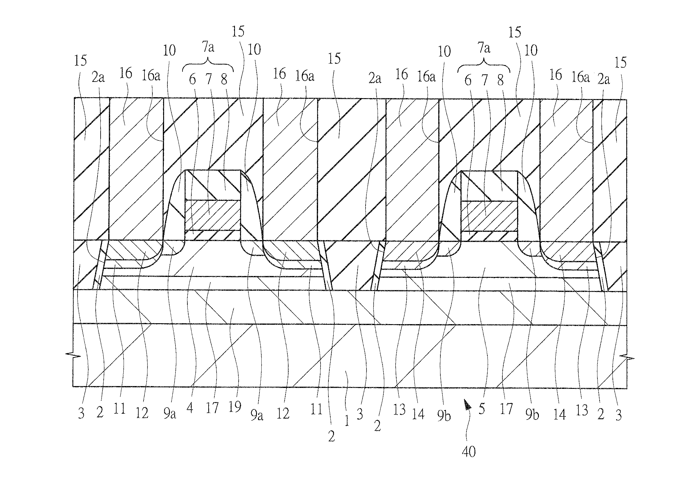
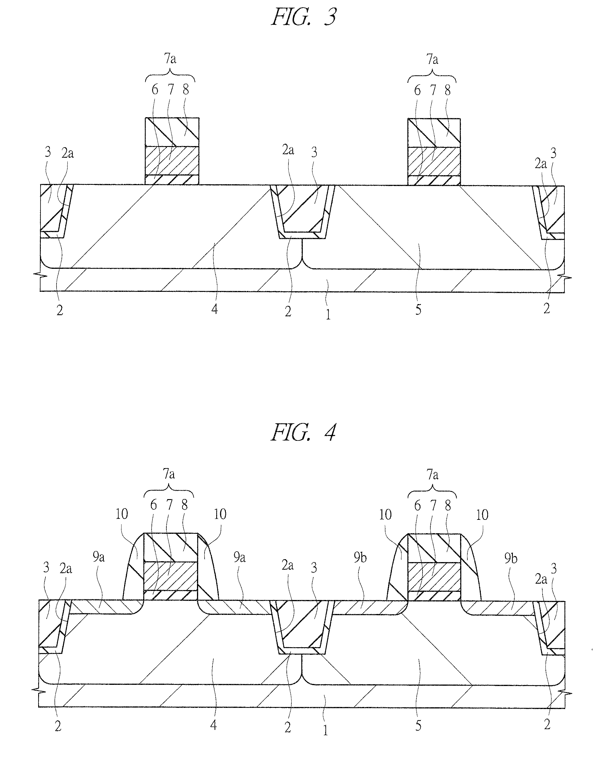
[0042]The present embodiment is applied to a manufacturing method of a CMIS, and will be described with reference to FIGS. 1 to 12.

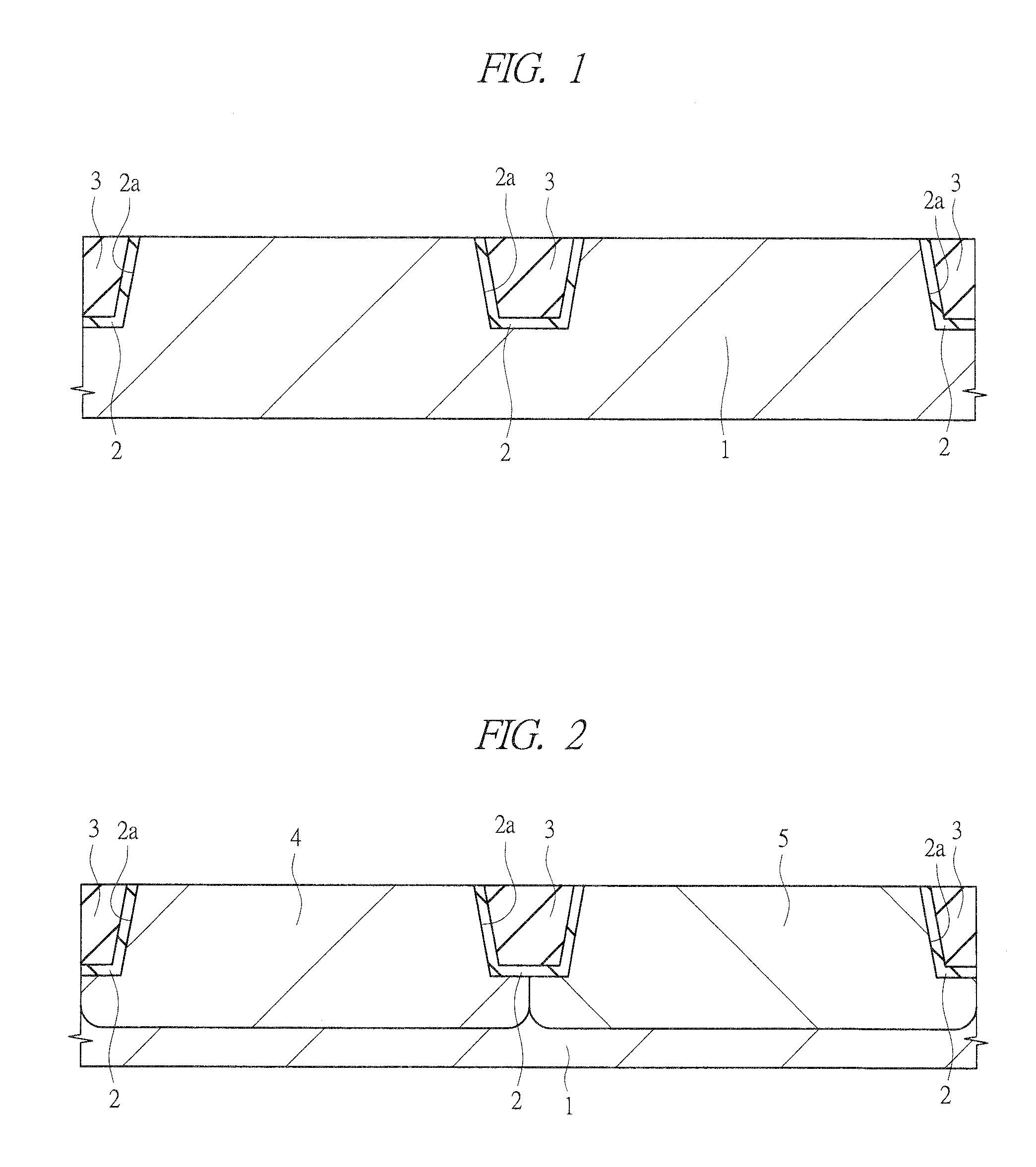
[0043]First, as illustrated in FIG. 1, shallow trenches 2a are formed in a main surface of a silicon substrate 1, and an inside of the shallow trench 2a is thermally oxidized at temperature of about 1000° C. to form a thermal oxide film 2 having a thickness of 5 to 20 nm. And then, a buried oxide film 3 is deposited inside the shallow trench 2a by a CVD method or a sputtering method, and then, annealing is performed for one to two hours at 1000 to 1150° C. under a diluted oxidizing atmosphere or a nitrogen atmosphere to densify the buried oxide film 3 aiming at reducing its voids. Further, excessive buried oxide film 3 on the silicon substrate 1 is removed to be flattened by CMP or etch-back, so that a device isolation structure is formed.

[0044]Next, as illustrated in FIG. 2, a surface of the silicon substrate 1 is thermally processed at 900° C. under an...

second embodiment

[0061]In recent years, efforts to improve electric properties have been made by depositing a layer including SiGe on a semiconductor substrate such as a strained Si substrate and forming a Si epitaxial layer on the layer to give a strain caused from SiGe to the Si epitaxial layer. This is because the strained Si has a high electron mobility, so that the operation speed of a device such as an LSI can be improved. In the present embodiment, a CMIS having a SiGe layer will be described.

[0062]First, as illustrated in FIG. 13, a SiGe layer 17 is formed on a silicon substrate 1 by an IBS (ion beam sputtering) method, and a silicon layer 18 is formed on the SiGe layer 17 by epitaxial growth.

[0063]Next, while a device isolation structure is formed in the silicon layer 18, processes after this formation are performed similarly to those of the first embodiment.

[0064]That is, first, the device isolation structure formed of a thermal oxide film 2 and a buried oxide film 3 is formed in the silic...


PUM


Abstract

Generation of dislocation and increase of diffusion resistance at edge portions of source/drain regions in a CMIS are prevented. When source/drain regions in a CMIS are formed, argon is implanted to a P-well layer as a dislocation-suppressing element and nitrogen is implanted to an N-well layer as a dislocation-suppressing element before an ion implantation of impurities to a silicon substrate. In this manner, by separately implanting dislocation-suppressing elements suitable for each of the P-well layer and the N-well layer as well as suppressing the generation of dislocation, increase of diffusion resistance can be suppressed, yield can be improved, and the reliability of devices can be increased.

Description

CROSS-REFERENCE TO RELATED APPLICATION[0001]The present application claims priority from Japanese Patent Application No. JP 2008-309727 filed on Dec. 4, 2008, the content of which is hereby incorporated by reference into this application.TECHNICAL FIELD OF THE INVENTION[0002]The present invention relates to a semiconductor device and a manufacturing method of the same. More particularly, the present invention relates to a technique effectively applied to a semiconductor device having a CMIS structure and a manufacturing method of the same.BACKGROUND OF THE INVENTION[0003]Impurities such as As (arsenic), P (phosphorus), or B (boron) (BF2) are implanted with a high dose to source and drain regions to be gate end portions of a MIS transistor (hereinafter, simply called MIS). Since the gate end portion is a portion to which stress is concentrated, dislocation is caused in a vicinity of the gate end portion often. Since the cause of dislocation becomes a source of leakage current, disloc...

Claims


Application Information

Patent Timeline
IPC IPC(8): H01L27/12H01L21/86
CPCH01L21/26506H01L21/26513H01L21/823814H01L29/6659H01L21/84H01L27/1203H01L29/1054H01L21/823892
Inventor ISHITSUKA, NORIOOHTA, HIROYUKIKIMURA, YASUHIROYAMAGUCHI, NATSUOTAKEUCHI, TAKASHIYOSHIDA, SHOJI
Owner RENESAS ELECTRONICS CORP
Why Eureka
Try Eureka