

Optical element module and method of manufacturing the same
a technology of optical elements and modules, applied in the direction of optical elements, instruments, optical waveguide light guides, etc., can solve the problems of package independent of optical fibers, damage to members incorporated in advance thereof, and inability to manufacture the same,
- Summary
- Abstract
- Description
- Claims
- Application Information
AI Technical Summary
Benefits of technology
Problems solved by technology
Method used
Image

Examples
first embodiment
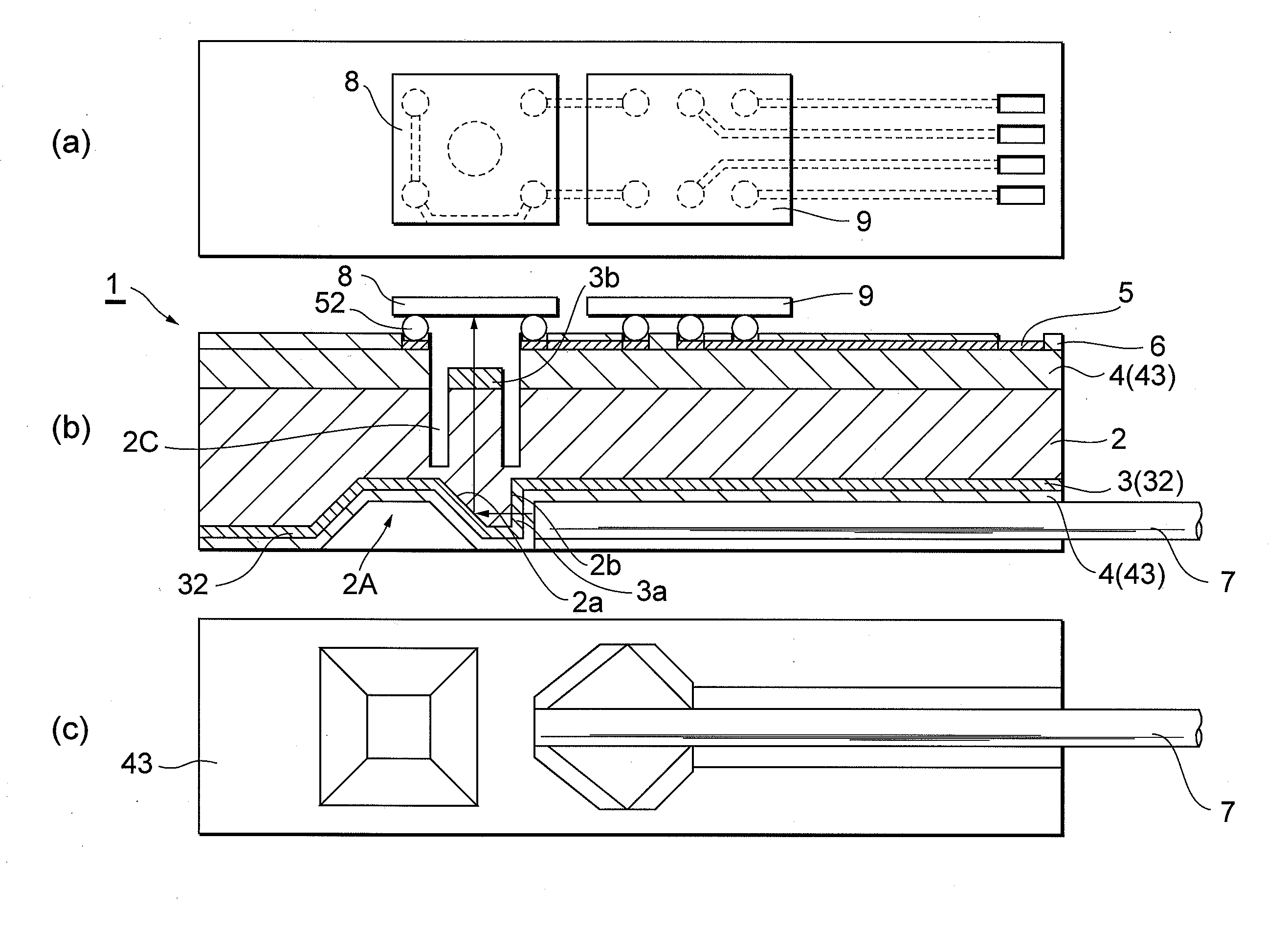
[0044]FIGS. 1 to 13 are diagrams for explanation of a method of manufacturing according to the present invention. Note that, in the respective drawings, views (a) show respective front surfaces viewed from above, views (b) show respective longitudinal sections in their central parts, and views (c) show rear surfaces viewed from underneath.
[0045]First, a completed optical element module 1 will be described with reference to FIG. 13. A silicon oxide film (SiO2) 4 serving as an insulating film is formed on a front surface of a silicon substrate 2, and a metal wiring 5 having a predetermined shape is disposed on an upper surface thereof. A passivation film 6 is formed on an upper surface of the metal wiring, and the metal wiring 5, and an optical element 8 and a semiconductor circuit element 9 are electrically connected via bumps 52 located at openings of the passivation film.
[0046]The optical element 8 is a light receiving element such as a photodiode or a light emitting element such a...
second embodiment
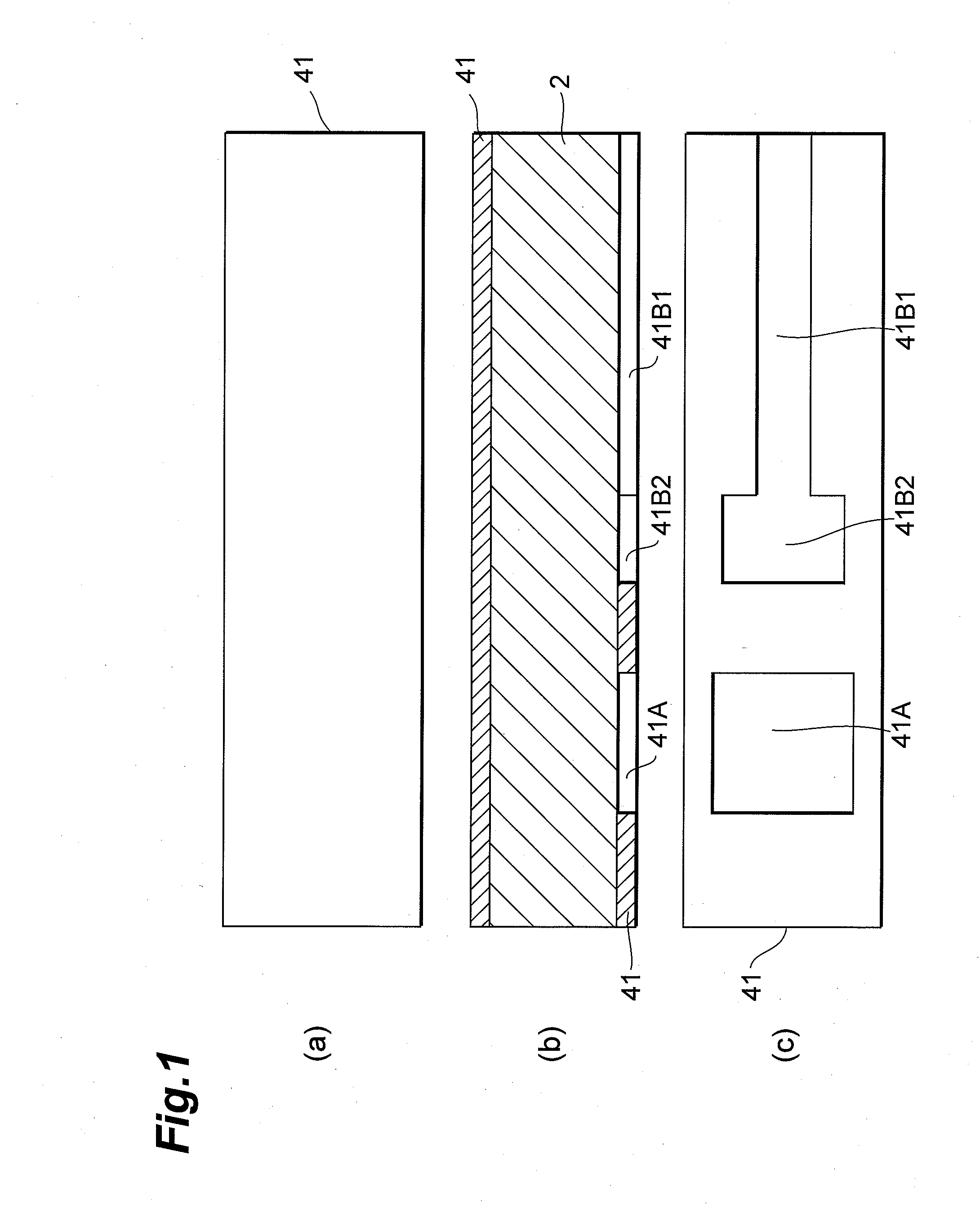
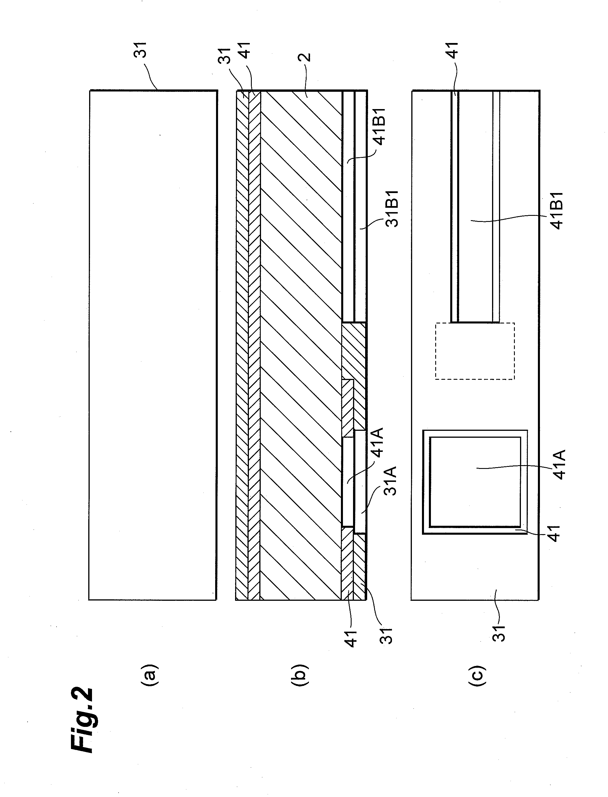
[0057]In the first crystal anisotropic etching, etching to make an appearance of a {110} plane is performed by use of EPW (a mixed liquid of ethylenediamine, pyrocatechol, and water) or hydrazine (N2H4.H2O) as an etchant. It is possible to form a {110} plane by use of a mixed liquid of potassium hydroxide (KOH) and isopropyl alcohol (IPA) as well, as an etchant. In the present embodiment, the silicon oxide film is used as a mask for the rims of the openings 41A and 41B1, and the silicon oxide film is eroded by KOH. Therefore, in the case in which a mixed liquid of KOH and IPA is used, it is preferable that the silicon oxide film is made to have a thickness of 0.5 μm or more with respect to etching of 100 μm, to be a thick silicon oxide film, or the silicon oxide film 41 is covered with the silicon nitride film 31 as in a second embodiment which will be described later, which makes the silicon nitride film 31 function as a mask.
[0058]Here, not only the mirror surface 2a, but also the...
PUM
 Abstract
Description
Claims
Application Information