Thin-film transistor substrate and method of fabricating the same

a thin film transistor and substrate technology, applied in the field of thin film transistors, can solve the problems of deterioration of tft substrate properties, low charge mobility and on/off current ratio, and low charge mobility of hydrogenated amorphous silicon, so as to reduce appearance defects and improve electrical properties

Active Publication Date: 2010-06-17
SAMSUNG DISPLAY CO LTD
View PDF17 Cites 70 Cited by
  • Summary
  • Abstract
  • Description
  • Claims
  • Application Information

AI Technical Summary

Benefits of technology

[0009]In an exemplary embodiment, a thin-film transistor (TFT) substrate

Problems solved by technology

Disadvantageously, hydrogenated amorphous silicon has a relatively low charge mobility and on/off current ratio.
In addition, since hydrogenated amorphous silicon has a small optical band gap, leakage photocurrent is generated from a backlight unit, and an afterimage is created due to an in

Method used


Image

  • Thin-film transistor substrate and method of fabricating the same
  • Thin-film transistor substrate and method of fabricating the same
  • Thin-film transistor substrate and method of fabricating the same

Examples


second embodiment

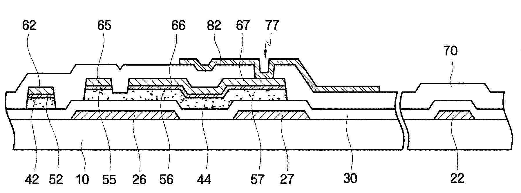
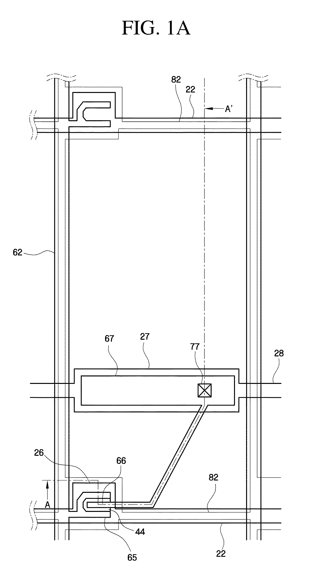
[0068]Referring to FIGS. 6A through 6C, the oxide of the first material of the oxide active layer patterns 42 and 44 included in the TFT substrate does not react with the second material of the buffer layer patterns 52 and 55 through 57.

[0069]In the TFT substrate according to the second embodiment, gallium indium zinc oxide (GaInZnO), hafnium indium zinc oxide (HfInZnO), or zinc oxide (ZnO) is used for the oxide active layer patterns 42 and 44, molybdenum is used for the buffer layer patterns 52 and 55 through 57, and copper or aluminum is used for the data wiring. Each of FIGS. 6A through 6C illustrates whether the oxide of the first material reacts with the second material when gallium indium zinc oxide (GaInZnO), hafnium indium zinc oxide (HfInZnO), or zinc oxide (ZnO) (respectively) is used as the oxide of the first material and a sufficient amount of molybdenum is used as the second material. In FIGS. 6A through 8C, a molar ratio of gallium to indium to zinc is set to 2:2:1, a...

first embodiment

[0078]Referring to FIG. 11, a conductive layer 60 for forming data wiring is deposited on the buffer layer 50 by, for example, sputtering. Then, the conductive layer 60 is coated with a photoresist layer 110. The conductive layer 60 according to the present embodiment may be identical to the material of the data wiring (not shown) and may contain aluminum or copper. The conductive layer 60 for the data wiring is deposited at a low temperature, i.e., of 80 to 100° C. When the conductive layer 60 is formed at low temperature, the oxide active layer 40 is prevented from reacting with the buffer layer 50. Thus, the first material included in the oxide active layer 40 is not intercalated into the conductive layer 60.

[0079]Referring to FIG. 12, the photoresist layer 110 is exposed to light by using a mask and then developed to form photoresist layer patterns 112 and 114. The photoresist layer pattern 114 is disposed over a channel region of a TFT, that is, disposed in a region between a ...


PUM


Abstract

A thin-film transistor (TFT) substrate has improved electrical properties and reduced appearance defects and a method of fabricating the TFT substrate, are provided. The TFT substrate includes: gate wiring which is formed on a surface of an insulating substrate; oxide active layer patterns which are formed on the gate wiring and include an oxide of a first material; buffer layer patterns which are disposed on the oxide active layer patterns to directly contact the oxide active layer patterns and include a second material; and data wiring which is formed on the buffer layer patterns to insulatedly cross the gate wiring, wherein a Gibbs free energy of the oxide of the first material is lower than a Gibbs free energy of an oxide of the second material.

Description

[0001]This application claims priority to Korean Patent Application No. 10-2008-0128678, filed on Dec. 17, 2008, and all the benefits accruing therefrom under 35 U.S.C. 119, the disclosure of which is incorporated herein by reference in its entirety.BACKGROUND OF THE INVENTION[0002]1. Field of the Invention[0003]The present invention relates to a thin-film transistor (“TFT”) substrate and a method of fabricating the same, and more particularly, to a TFT substrate which has improved electrical properties and reduced appearance defects and a method of fabricating the TFT substrate.[0004]2. Description of the Related Art[0005]Liquid crystal displays (“LCDs”) are one of the most widely used flat panel displays (“FPDs”). An LCD includes two substrates having electrodes formed thereon and a liquid crystal layer interposed between the two substrates. In the LCD, voltages are applied to the electrodes to rearrange aligned liquid crystal molecules of the liquid crystal layer and thereby cont...

Claims


Application Information

Patent Timeline
IPC IPC(8): H01L29/786H01L21/336
CPCH01L27/12H01L27/1225H01L29/45H01L27/124H01L29/7869H01L29/66969H01L29/78618G02F1/1368H01L27/1214H01L29/458H01L29/66742
Inventor KIM, DO-HYUNYUN, PIL-SANGKIM, KI-WONLEE, DONG-HOONJEONG, CHANG-OH
Owner SAMSUNG DISPLAY CO LTD
Why Eureka
Try Eureka