Field effect transistor with electric field and space-charge control contact

a field effect transistor and electric field technology, applied in the field of transistors, can solve the problems of insufficient compact and efficient transistor thz devices, device bulkiness, and electronic devices such as photomixers and frequency multipliers cannot deliver radio frequency (rf) power in the micro-watt rang

Active Publication Date: 2010-06-24
SENSOR ELECTRONICS TECH
View PDF34 Cites 30 Cited by
  • Summary
  • Abstract
  • Description
  • Claims
  • Application Information

AI Technical Summary

Benefits of technology

[0013]A first aspect of the invention provides a device comprising: a field effect transistor including: a device conducting channel; a source contact, a drain contact, and a gate contact to the device conducting channel; a first isolation layer over the source contact, wherein the first isolation layer extends beyond the source contact into only a portion of a spacing between the source contact and the gate contact; and a first capacitive contact to the device conducting channel over the first isolation layer, wherein at least a portion of the first capacitive contact is located within only a portion of the spacing between the source contact and the gate contact and wherein the first capacitive contact is isolated from the source contact by the first isolation layer.
[0014]A second aspect of the invention provides a circuit comprising: a field effect transistor including: a device conducting channel; a source contact, a drain contact, and a gate contact to the device conducting channel; a first isolation layer over the source contact, wherein the first isolation layer extends beyond the source contact into only a portion of a spacing between the source contact and the gate contact; and a first capacitive contact to the device con...

Problems solved by technology

In spite of great demand for efficient THz devices, compact and efficient transistor THz devices are not yet available.
Achieving electronic device operation in the THz range is a complex multifaceted problem involving the control of electron velocity, electric field and potential profiles, access resistances, parasitic parameters, and electromagnetic coupling.
To date, electronic devices such as photomixers and frequency multipliers can only deliver radio frequency (RF) powers in the micro-watt range when operating at frequencies in the THz range.
Electronic THz lasers can emit high powers, e.g., up to one Watt, however, these devices are bulky, require high pumping powers and cannot be fabricated using integrated technology.
However, to date, high power THz operation has not been achieved.
Key obstacles to providing high power, high frequency operation include relatively low current density in Si, GaAs and InP based devices, rapid degradation of cutof...

Method used


Image

  • Field effect transistor with electric field and space-charge control contact
  • Field effect transistor with electric field and space-charge control contact
  • Field effect transistor with electric field and space-charge control contact

Examples


Embodiment Construction

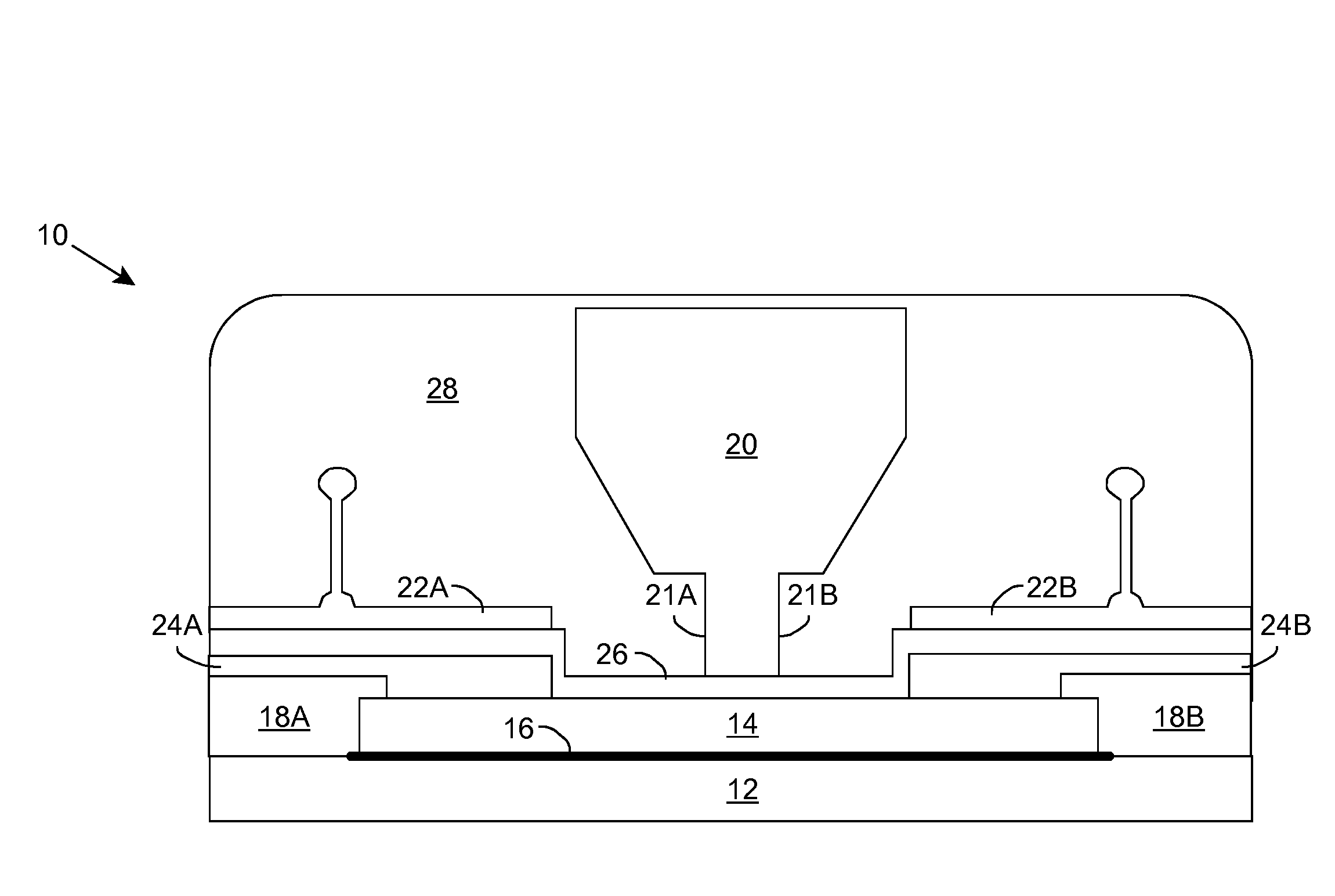
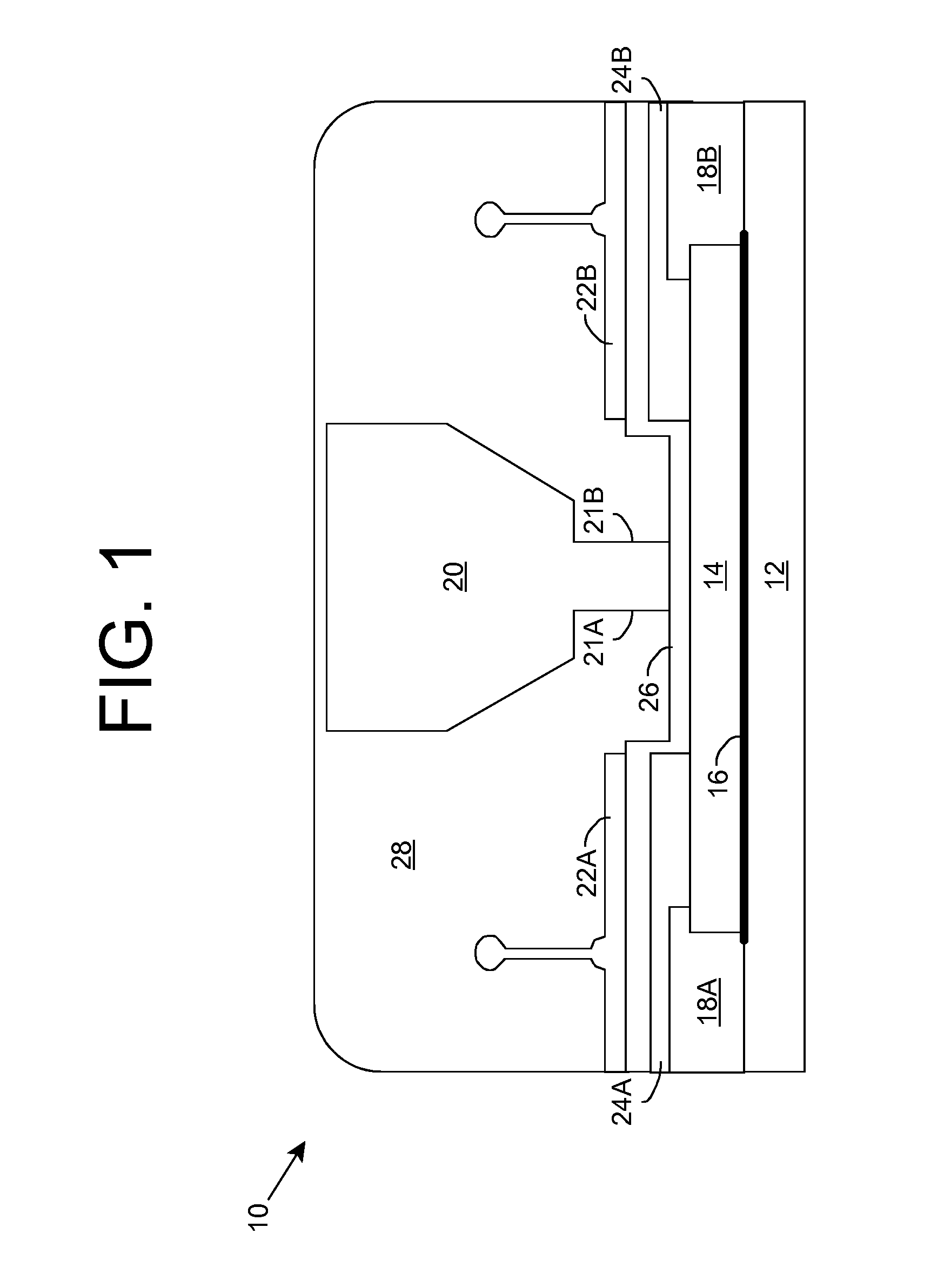
[0025]As indicated above, aspects of the invention provide a group III nitride-based device capable of achieving terahertz-range cutoff and maximum frequencies of operation at relatively high drain voltages. In an embodiment, two additional independently biased electrodes are used to control the electric field and space-charge close to the gate edges. As a result, an effective gate length extension due to short channel effects is diminished and electron velocity in the device channel is increased. It is understood that for the purposes of the disclosure, Al means Aluminum, As means Arsenic, Ga means Gallium, Hf means Hafnium, In means Indium, O means Oxygen, N means Nitrogen, and Si means Silicon. As used herein, unless otherwise noted, the term “set” means one or more (i.e., at least one) and the phrase “any solution” means any now known or later developed solution.

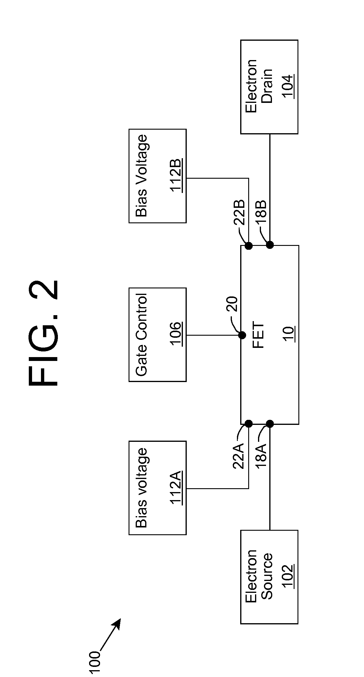
[0026]Turning to the drawings, FIG. 1 shows an illustrative device 10 according to an embodiment. Device 10 includes a...


PUM


Abstract

A group III nitride-based transistor capable of achieving terahertz-range cutoff and maximum frequencies of operation at relatively high drain voltages is provided. In an embodiment, two additional independently biased electrodes are used to control the electric field and space-charge close to the gate edges.

Description

REFERENCE TO PRIOR APPLICATIONS[0001]The current application claims the benefit of co-pending U.S. Provisional Application No. 61 / 203,433, titled “5-Terminal THz GaN based transistor with field- and space-charge control electrodes”, which was filed on 23 Dec. 2008, and which is hereby incorporated by reference.[0002]Aspects of the application are also related to co-pending U.S. Utility application Ser. No. 11 / 781,302, titled “Composite contact for semiconductor device”, which was filed on 23 Jul. 2007, co-pending U.S. Utility application Ser. No. 11 / 781,308, titled “Fabrication of semiconductor device having composite contact”, which was filed on 23 Jul. 2007, and co-pending U.S. Utility application Ser. No. 11 / 781,338, titled “Enhancement mode insulated gate heterostructure field-effect transistor”, which was filed on 23 Jul. 2007, each of which is hereby incorporated by reference.TECHNICAL FIELD[0003]The disclosure relates generally to transistors, and more particularly, to a nitr...

Claims


Application Information

Patent Timeline
IPC IPC(8): H03B1/00H01L29/12H01L27/06
CPCH01L29/7786H01L29/2003
Inventor SIMIN, GRIGORYSHUR, MICHAELGASKA, REMIGIJUS
Owner SENSOR ELECTRONICS TECH
Why Eureka
Try Eureka