
Chip antenna and its production method, and antenna apparatus and communications apparatus comprising such chip antenna

a technology of chip antenna and production method, which is applied in the direction of inductance with magnetic core, filament/thread forming, fibre treatment, etc., can solve the problems that the ferrite-made antenna cannot be sufficiently small and operable in a wide band, and achieve the effect of improving reliability

Inactive Publication Date: 2010-06-24
HITACHI METALS LTD
View PDF11 Cites 22 Cited by
  • Summary
  • Abstract
  • Description
  • Claims
  • Application Information

AI Technical Summary

Benefits of technology

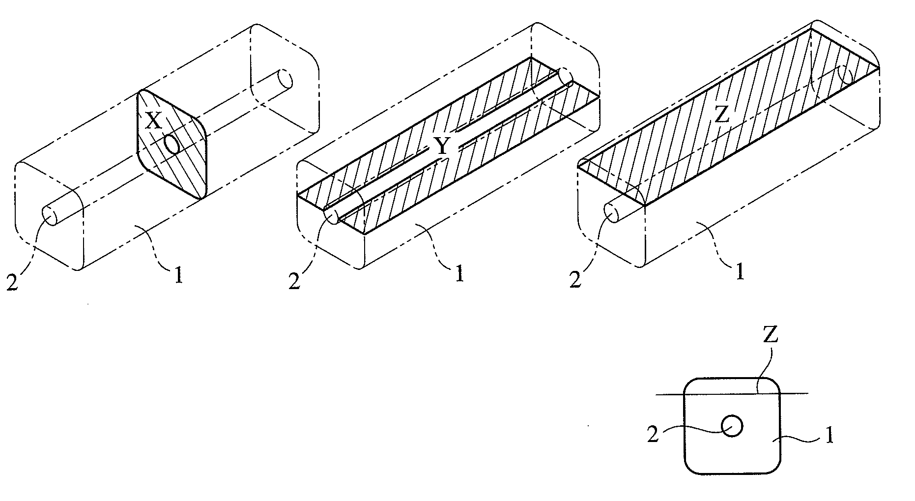
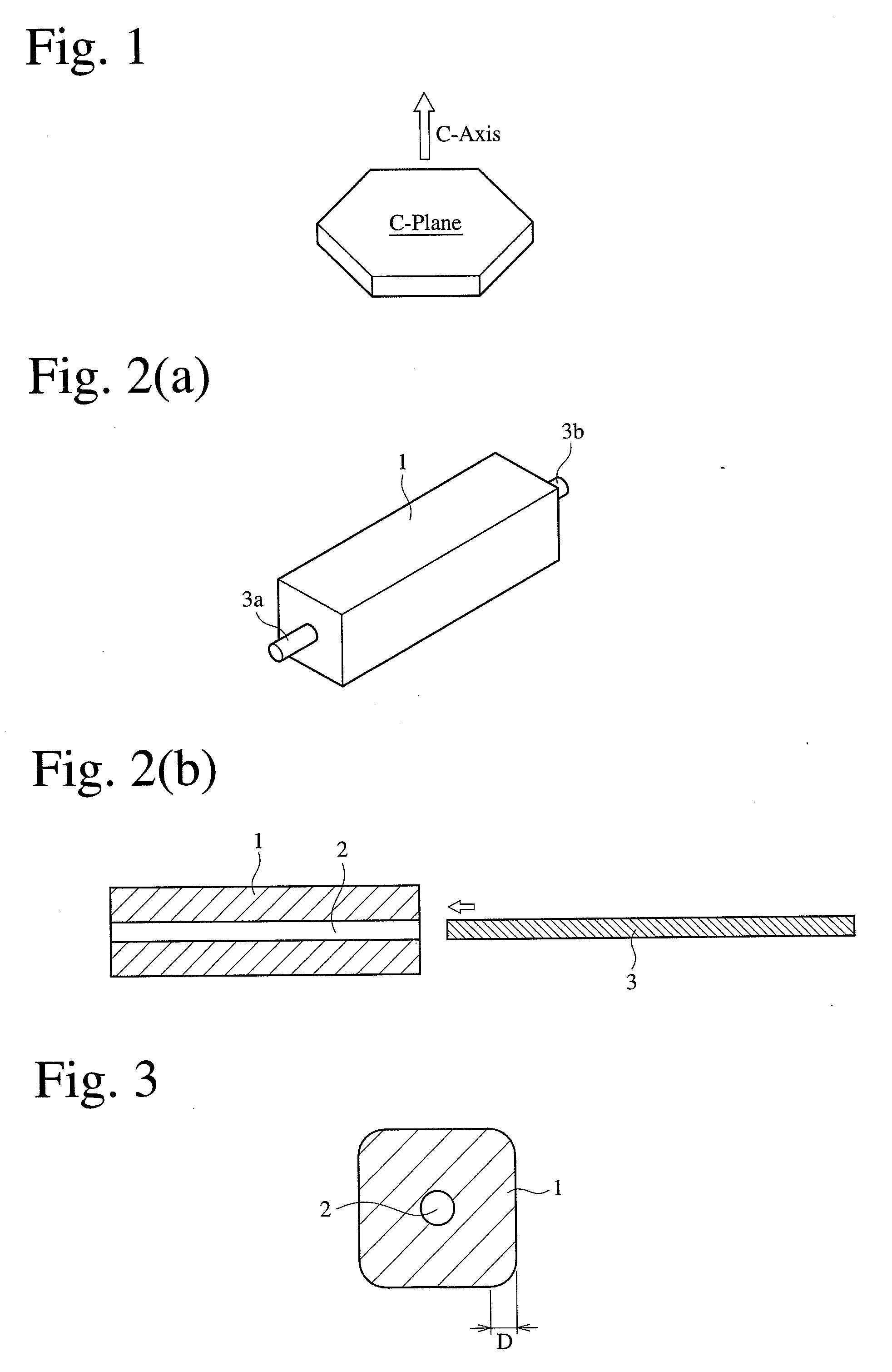
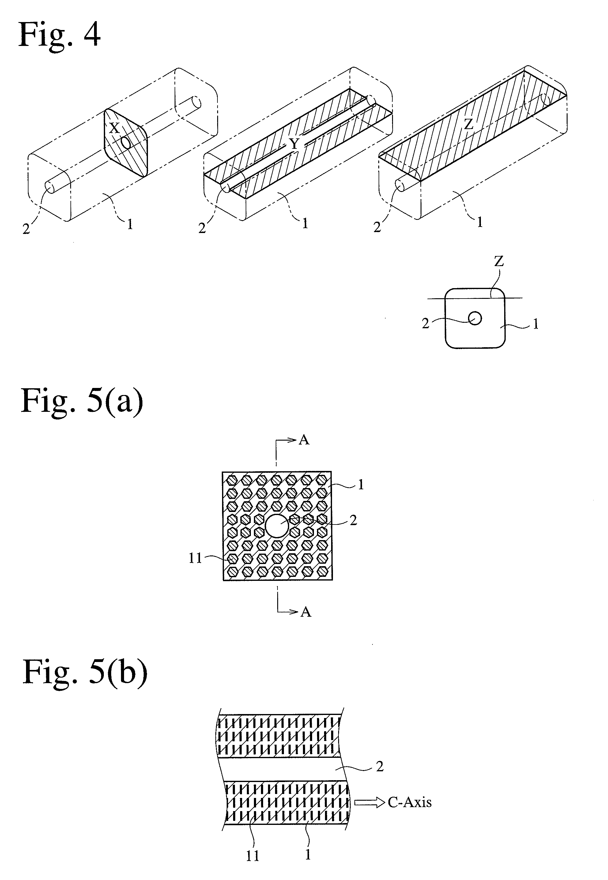
[0007]Each of the first and second chip antennas is small and operable in a wide band, because the conductor penetrating the linear through-hole does not have portions opposing to each other, so that a magnetic body can effectively function as inductance. Because the c-axis (difficult magnetization axis) of Z-type ferrite or Y-type ferrite is oriented substantially parallel or perpendicular to the through-hole, initial permeability is aligned in a circumferential direction around the linear through-hole. Accordingly, a magnetic field generated by the linear conductor can be utilized efficiently, making it possible to miniaturize the antenna.
[0013]Conductors in pluralities of chip antennas may be connected in series to constitute a chip antenna assembly. With series-connected conductors bent, the arrangement of pluralities of magnetic substrates can be changed according to a mounting space. Thus, the antennas can be assembled in communications apparatuses, etc. with high space efficiency. Further, because individual magnetic substrates can be made shorter relative to chip antenna length necessary for antenna characteristics, the shock resistance of the entire chip antenna is increased.
[0015]The communications apparatus of the present invention comprises the above antenna apparatus. Because the above antenna apparatus functions in a wide band, the communications apparatus comprising it can also be used in a wide band. The above antenna apparatus is suitable for portable terminals for digital terrestrial broadcasting, cell phones, etc., contributing to miniaturization and the improvement of reliability.

Problems solved by technology

However, even a ferrite-made antenna cannot be sufficiently small and operable in a wide band, unless having a structure effectively providing inductance while suppressing a capacitance component.

Method used


Image

  • Chip antenna and its production method, and antenna apparatus and communications apparatus comprising such chip antenna
  • Chip antenna and its production method, and antenna apparatus and communications apparatus comprising such chip antenna
  • Chip antenna and its production method, and antenna apparatus and communications apparatus comprising such chip antenna

Examples


example 1

[0067]100 parts by mass of main components comprising Fe2O3, BaCO3 and CO3O4 in such proportions that Fe2O3 was 70.2% by mol, BaO was 18.8% by mol, and CoO was 11.0% by mol were mixed with 3.0 parts by mass of Mn3O4, 0.4 parts by mass of Li2CO3 and 0.13 parts by mass of SiO2 for 16 hours by wet ball milling, and calcined at 1200° C. for 2 hours in the air. The calcined powder was pulverized for 18 hours by wet ball milling, and then granulated with a binder (PVA). The granulated powder was sintered at 1300° C. for 3 hours in the air. The sintered body was pulverized a jaw crusher, a disc mill and a vibration mill. The resultant sintered powder had a specific surface area of 10800 cm2 / g (measured by a BET method using Model-1201 available from Macsorb).

[0068]Pure water was added to the sintered powder to prepare slurry having a concentration of 75% by mass, which was wet-molded to a ring shape (Sample 1) and a rectangular shape (Sample 2) under pressure of 25 MPa while applying a rot...

example 2

[0070]100 parts by mass of main components comprising Fe2O3, BaCO3 and CO3O4 in such proportions that Fe2O3 was 60% by mol, BaO was 19.5% by mol, and CoO was 20.5% by mol were mixed with 0.6 parts by mass of CuO for 16 hours by wet ball milling with water as a medium. The mixed powder was dried, and then calcined at 1000° C. for 2 hours in the air. The calcined powder was pulverized for 18 hours by wet ball milling with water as a medium. 100 parts by mass of the resultant powder was mixed with 1% by mass of binder (PVA) for granulation, and pressed to a ring shape. The resultant green body was sintered at 1200° C. for 3 hours in the air to form a ring-shaped, sintered body (Sample 2) having an outer diameter of 7.0 mm, an inner diameter of 3.5 mm and a height of 3.0 mm, and a rectangular sintered body (Sample 3) of 10 mm×3 mm×3 mm having a through-hole having a circular cross section of 0.6 mm in diameter along a center axis. X-ray diffraction revealed that the main phase of the si...

example 3

[0071]100 parts by mass of main components comprising Fe2O3, BaCO3 and CO3O4 in such proportions that Fe2O3 was 60% by mol, BaO was 19.5% by mol, and CoO was 20.5% by mol were mixed with 0.6 parts by mass of CuO by wet ball milling with water as a medium. The mixed powder was dried, and then calcined at 1100° C. for 1.5 hours in the air. The calcined powder was pulverized for 10 hours by wet ball milling with water as a medium, and mixed with water, a binder, a lubricant and a plasticizer to prepare a moldable material having a water content of 13.8% by mass. Using a die shown in FIG. 8, the moldable material was extruded, dried, and sintered at 1150° C. for 3 hours in the air to form a rectangular sintered body (Sample 4) of 10 mm×3 mm×3 mm having a through-hole having a circular cross section of 0.6 mm in diameter along a center axis, and a chamfered curve surface of 0.5 mm in width at each corner. X-ray diffraction revealed that the main phase of the sintered body was Y-type ferr...


PUM

PropertyMeasurementUnit
Depthaaaaaaaaaa
Magnetismaaaaaaaaaa

Abstract

A chip antenna comprising a magnetic substrate comprising Z-type ferrite or Y-type ferrite as a main phase and having a through-hole extending linearly along a center axis, and a conductor penetrating the through-hole, the magnetic phase having a c-axis substantially parallel or perpendicular to the through-hole.

Description

FIELD OF THE INVENTION[0001]The present invention relates to a small chip antenna suitable for communications apparatuses having wide operating frequency bands, such as cell phones, mobile terminal gears, etc., its production method, and an antenna apparatus and a communications apparatus comprising such chip antenna.BACKGROUND OF THE INVENTION[0002]Antennas in mobile communications apparatuses such as cell phones, wireless LAN, etc., which are used in as wide frequency bands as several hundreds of MHz to several GHz (for instance, 470-770 MHz in digital terrestrial broadcasting), are required to have high gain in such wide frequency bands, and small sizes with low height. As a small antenna suitable for such mobile communications apparatuses, JP 49-40046 A proposes an antenna which is made smaller by using a magnetic material having large dielectric constant ∈r and specific permeability μr to reduce wavelength to 1 / (∈r·μr)1 / 2, and JP 9-507828 A describes that sintered hexagonal fer...

Claims


Application Information

Patent Timeline
IPC IPC(8): H01Q1/00D01F1/08
CPCH01F17/06H01Q1/243H01Q1/2283
Inventor KATO, TOMOTSUGUGONDA, MASAYUKIAOYAMA, HIROYUKIMIKAMI, HIDETO
Owner HITACHI METALS LTD
Learn More