Gallium nitride-based compound semiconductor light emitting device

a compound semiconductor and light-emitting device technology, applied in the direction of semiconductor devices, basic electric elements, electrical equipment, etc., can solve the problems of low light extraction efficiency relative to generated light, low light extraction efficiency, and difficulty in saying that internal emitted light generated by injected current is adequately extracted to the outside, etc., to achieve superior light distribution uniformity, adequate emission output, and high emission output

Active Publication Date: 2010-07-15
TOYODA GOSEI CO LTD
View PDF14 Cites 23 Cited by
  • Summary
  • Abstract
  • Description
  • Claims
  • Application Information

AI Technical Summary

Benefits of technology

[0010]An object of the present invention is to solve the aforementioned problems of the prior art by providing a gallium nitride-based compound semiconductor light emitting device having superior light extraction efficiency and light distribution uniformity.
[0023]As a result of the bottom (substrate side) of the lateral surface being a reverse taper inclined at 5 to 85 degrees relative to the substrate main surface, and the top being a forward taper inclined at 95 to 175 degrees relative to the substrate main surface, the gallium nitride-based compound semiconductor light emitting device of the present invention has high emission output and superior light distribution uniformity. In particular, adequate emission output can be attained even if mounted in a special light emitting package having a reduced interval between the package lateral surface and light emitting device.

Problems solved by technology

However, in not only the case of GaN-based compound semiconductors, but also in the case of light emitting diodes (LED), the light extraction efficiency relative to generated light is generally low, and it is difficult to say that internally emitted light generated by injected current is adequately extracted to the outside.
The cause of low light extraction efficiency is that light emitted in an emission layer is repeatedly reflected and absorbed by the crystal material within the LED structure, and when that light is radiated outside the semiconductor layer, emitted light is not extracted to the outside due to reflection beyond the critical angle according to Snell's law, thereby resulting in the light being re-reflected within the crystal and lowering the probability of light reaching the outside.
However, when a gallium nitride-based compound semiconductor light emitting device having this inverted tapered lateral surface was mounted on a typical light emitting package, and the relationship between the emission angle and output characteristics was investigated, although a satisfactory emission output was obtained in the direction of the front surface due to light reflected by the inverted tapered lateral surface, adequate emission output was unable to be obtained where the emission angle is low, namely in the direction of the lateral surface of the light emitting diode, thereby demonstrating that light distribution uniformity is not satisfactory.
A light emitting device having an inverted tapered lateral surface as described above has been experimentally determined to not allow the obtaining of adequate device characteristics in these special light emitting packages utilizing light from the lateral surface of semiconductor light emitting device.

Method used


Image

  • Gallium nitride-based compound semiconductor light emitting device
  • Gallium nitride-based compound semiconductor light emitting device
  • Gallium nitride-based compound semiconductor light emitting device

Examples


examples

[0065]Although the following provides a detailed explanation of the present invention through examples and comparative examples thereof, the present invention is not limited to only these examples.

example

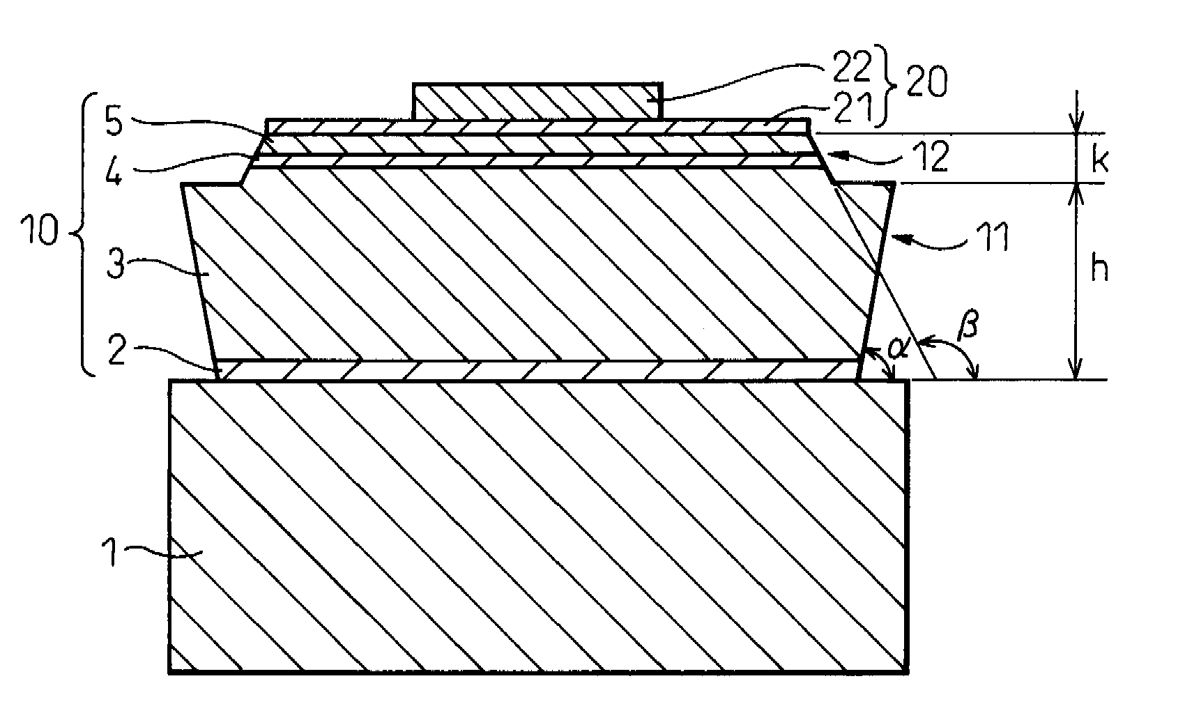
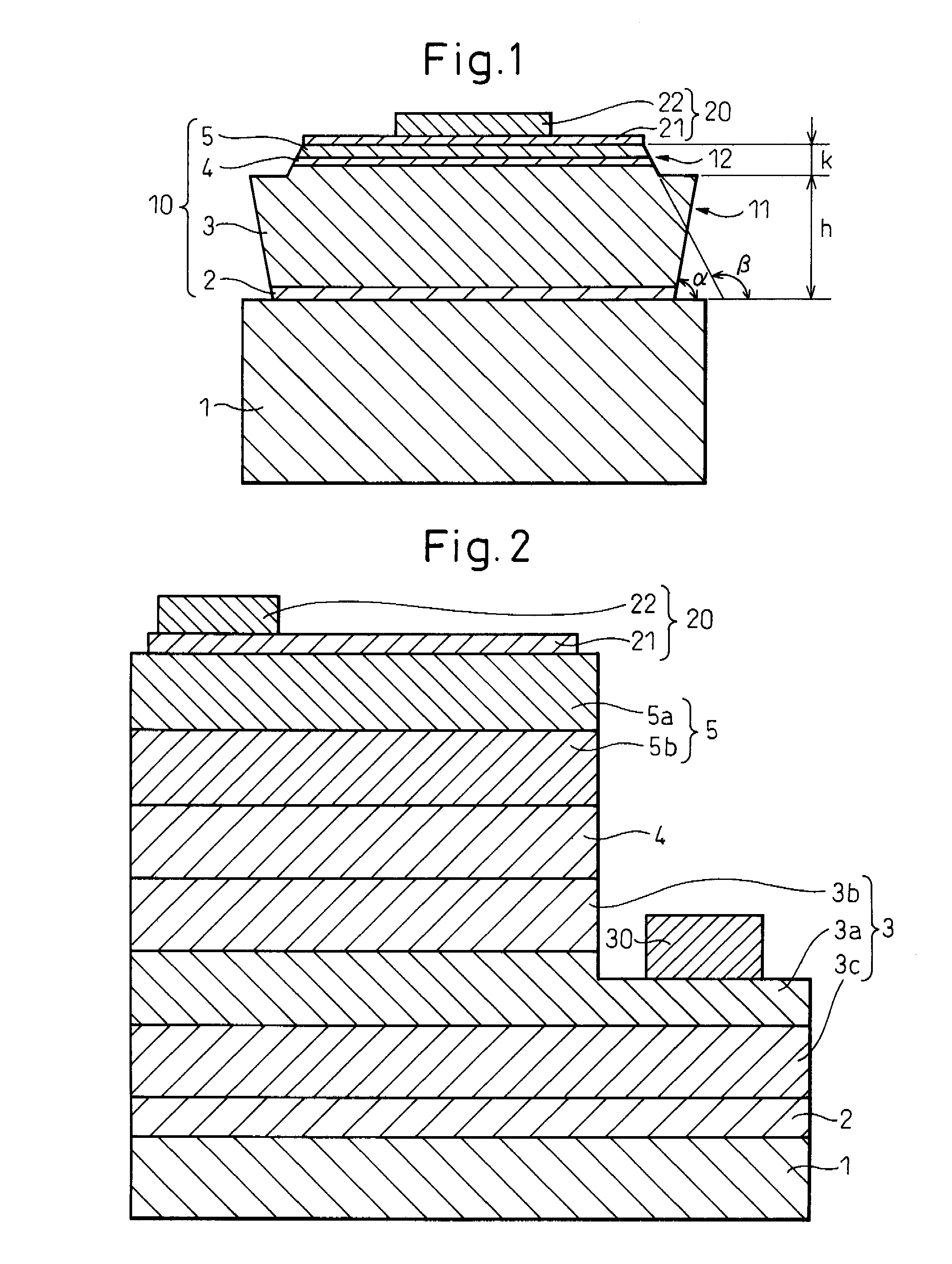
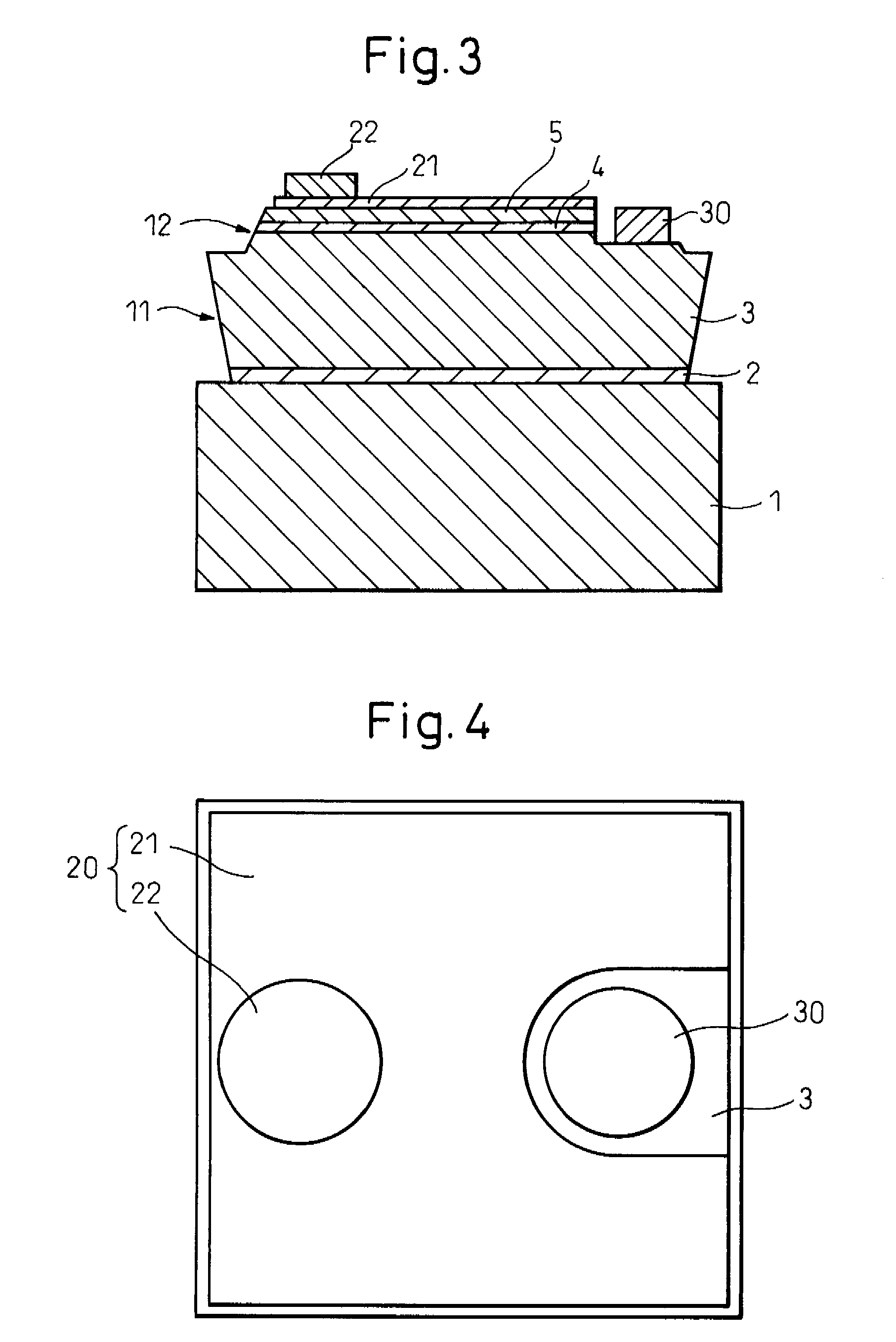
[0066]A cross-sectional schematic drawing of a gallium nitride-based compound semiconductor light emitting device fabricated in the present example is shown in FIG. 3. The stacked structure of the gallium nitride-based compound semiconductor is composed by sequentially stacking an n-type semiconductor layer 3, comprising an underlying layer composed of an undoped GaN layer (layer thickness=8 μm), an n-type contact layer composed of an Si-doped n-type GaN layer (layer thickness=2 μm, carrier concentration=1×1019 cm−3), and an n-type clad layer composed of an Si-doped Al0.07Ga0.93N layer (layer thickness=25 nm, carrier concentration=1×1018 cm−3), an emission layer 4, having a multiple quantum well structure in which six layers of an Si-doped GaN barrier layer (layer thickness=14.0 nm, carrier concentration=1×1018 cm−3) and five layers of an undoped In0.20Ga0.80N well layer (layer thickness=2.5 nm) are alternately stacked, and a p-type semiconductor layer 5, comprising a p-type clad la...


PUM


Abstract

An object of the present invention is to provide a gallium nitride-based compound semiconductor light emitting device having superior light extraction efficiency and light distribution uniformity.The inventive gallium nitride-based compound semiconductor light emitting device comprises a substrate and a gallium nitride-based compound semiconductor layer stacked on the substrate, wherein on at least one lateral surface of the light emitting device, the bottom (substrate side) of the semiconductor layer is a reverse taper inclined 5 to 85 degrees relative to the substrate main surface and the top of the semiconductor layer is a forward taper inclined 95 to 175 degrees relative to the substrate main surface.

Description

TECHNICAL FIELD[0001]The present invention relates to a gallium nitride-based compound semiconductor light emitting device, and more particularly, to a gallium nitride-based compound semiconductor light emitting device having superior emission output and light distribution uniformity.BACKGROUND ART[0002]Attention has recently been focused on GaN-based compound semiconductor light emitting devices as semiconductor materials for short wavelength light emitting devices. GaN-based compound semiconductors are formed by metal organic chemical vapor deposition (MOCVD) or molecular beam epitaxy (MBE) and the like on a substrate consisting of sapphire single crystal, various oxides or a group III-V compound.[0003]The external quantum efficiency of a light emitting device is expressed as the product of light extraction efficiency and internal quantum efficiency. Internal quantum efficiency refers to the proportion of electrical current energy injected into a light emitting device that is conv...

Claims


Application Information

Patent Timeline
Patent Type & Authority Applications(United States)
IPC IPC(8): H01L33/00H01L33/10H01L33/20H01L33/32
CPCH01L33/18H01L33/32H01L33/20
Inventor MURAKI, NORITAKAFUKUNAGA, NAOKI
Owner TOYODA GOSEI CO LTD
Why Eureka
Try Eureka