Semiconductor integrated circuit device and a method for manufacturing a semiconductor integrated circuit device

a technology of integrated circuit device and semiconductor, which is applied in the direction of semiconductor devices, semiconductor/solid-state device details, electrical apparatus, etc., can solve the problems of reducing reliability, unable to carry out probe testing on the pad electrode in the scribe region after rewiring formation, etc., and achieve the effect of improving the reliability of the devi

Inactive Publication Date: 2010-07-22
RENESAS ELECTRONICS CORP
View PDF5 Cites 50 Cited by
  • Summary
  • Abstract
  • Description
  • Claims
  • Application Information

AI Technical Summary

Benefits of technology

[0011]The present inventors conducted various studies on the wafer level package process in a method for manufacturing a semiconductor integrated circuit device. As a result, they found the following problems. Namely, in a general wafer level package process, in order to prevent the corrosion of aluminum type pad electrodes in a scribe region or the like in a plating process, the pad electrodes are covered with a resin film for pad protection at the same layer as a polyimide final passivation film in a product region. However, with this configuration, the probe test on the pad electrodes in the scribe region cannot be carried out after rewiring formation. Further, when blade dicing is performed, the polyimide final passivation film in the product region and the pad protective resin film are required to be separated from each other. As a result, the width of the scribe region increases. Still further, there is no polyimide final passivation film at the end of the product region, resulting in a reduction of the reliability, or the like.
[0018]Namely, in accordance with the present invention, in a method for manufacturing a semiconductor integrated circuit device (LSI) of a wafer level package system, an organic type final passivation film in the chip regions and an organic type final passivation film in the scribe region are mutually combined to form an integral film pattern. In a pelletization step, the surface layer portion including the organic type final passivation film at the central part of the scribe region is first removed by laser grooving, thereby to form a large-width groove. Then, the central part in this groove is subjected to a dicing processing (including a combined step with back grinding, or the like), resulting in separation into the chip regions. As a result, there occurs an organic type final passivation film integral up to the end of the top surface (device surface) of the chip. This improves the reliability of the device.

Problems solved by technology

As a result, they found the following problems.
However, with this configuration, the probe test on the pad electrodes in the scribe region cannot be carried out after rewiring formation.
Still further, there is no polyimide final passivation film at the end of the product region, resulting in a reduction of the reliability, or the like.

Method used


Image

  • Semiconductor integrated circuit device and a method for manufacturing a semiconductor integrated circuit device
  • Semiconductor integrated circuit device and a method for manufacturing a semiconductor integrated circuit device
  • Semiconductor integrated circuit device and a method for manufacturing a semiconductor integrated circuit device

Examples


Embodiment Construction

[0055][Outline of embodiments] First, the outline of typical embodiments of the present invention disclosed in the present application will be described.

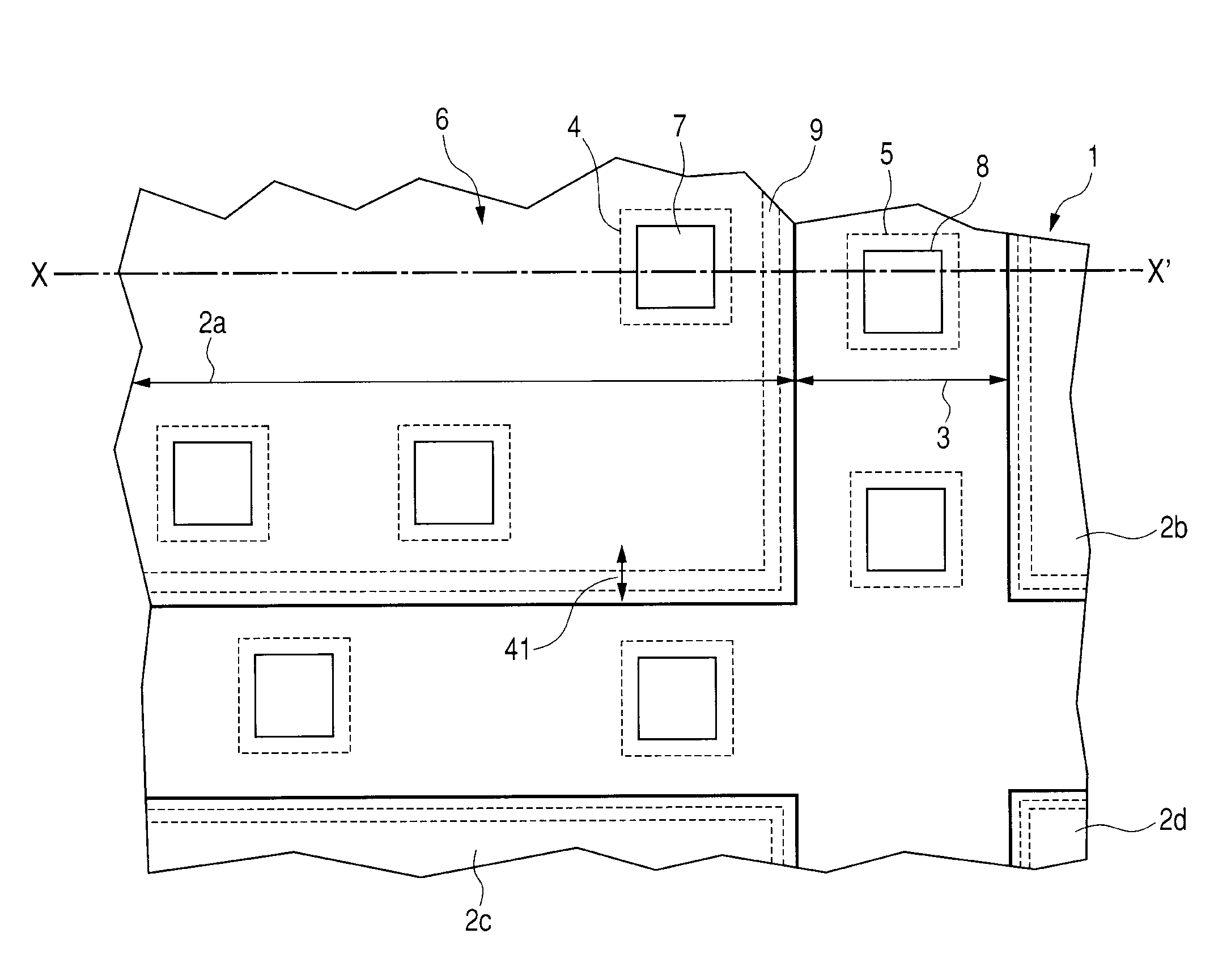
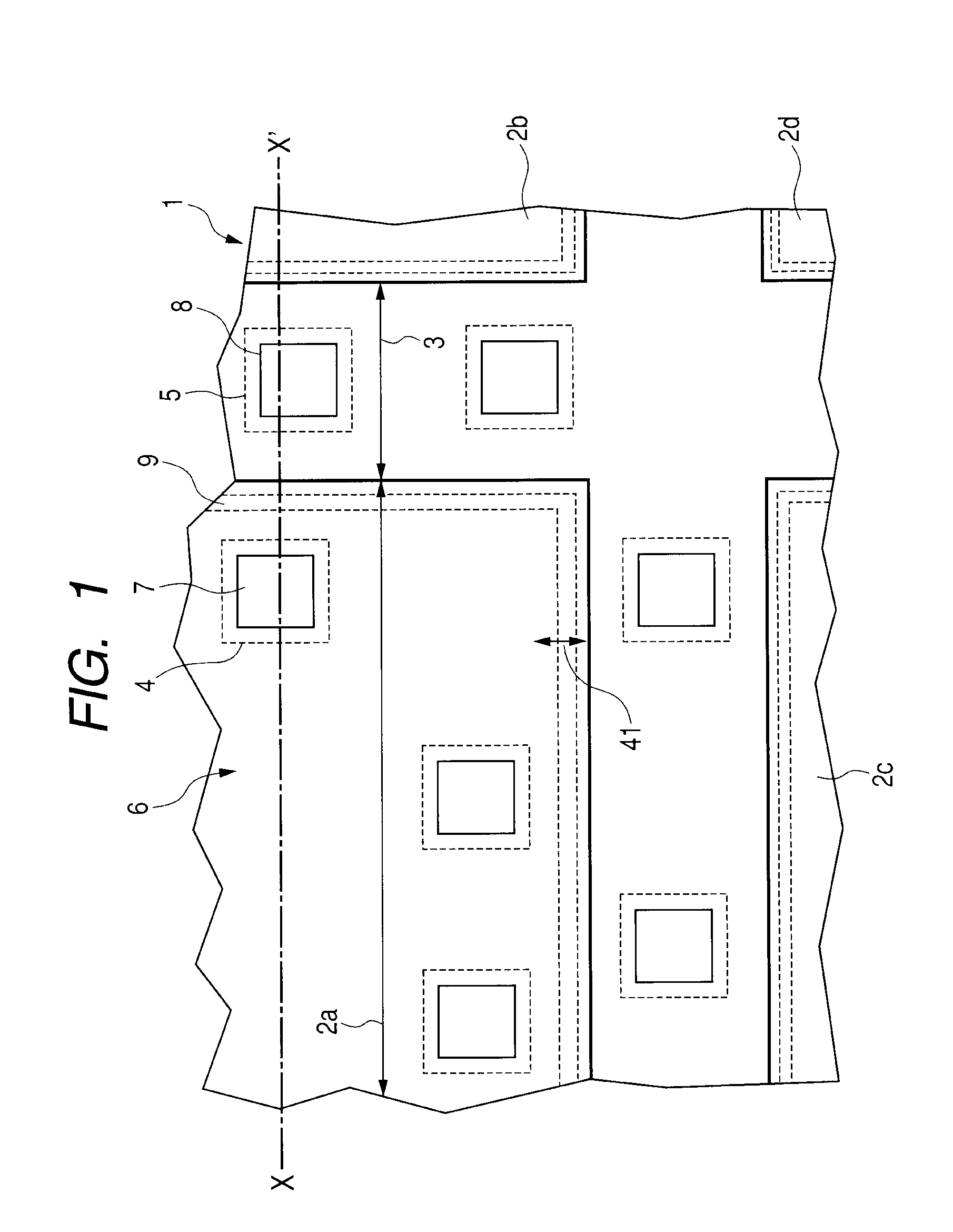
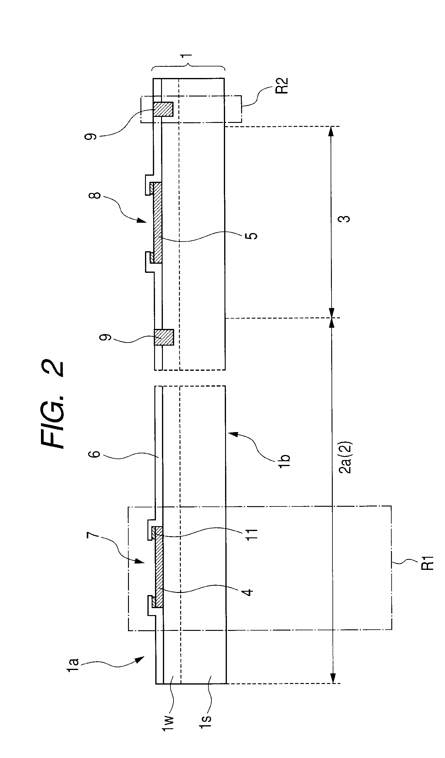
[0056]1. A method for manufacturing a semiconductor integrated circuit device, includes the steps of: (a) forming an on-chip rewiring pattern in each chip region over a device surface of a semiconductor wafer having a plurality of chip regions, and a scribe region therebetween, and forming a test rewiring pattern electrically coupled to an aluminum type pad electrode in the scribe region; (b) after the step (a), forming an organic type insulation film almost entirely over the device surface including the surface of the on-chip rewiring pattern; (c) forming a bump forming opening in the organic type insulation film over the on-chip rewiring pattern; (d) forming a bump electrode over the on-chip rewiring pattern at the bump forming opening; (e) after the step (d), carrying out a laser processing on the scribe region, and thereby remov...


PUM


Abstract

With a general wafer level package process, in order to prevent corrosion of an aluminum type pad electrode in a scribe region in a plating process, the pad electrode is covered with a pad protective resin film at the same layer as an organic type protective film in a product region. However, this makes it impossible to perform the probe test on the pad electrode in the scribe region after rewiring formation. The present invention provides a method for manufacturing a semiconductor integrated circuit device of a wafer level package system. The organic type protective films in the chip regions and the scribe region are mutually combined to form an integral film pattern. In a pelletization step, the surface layer portion including the organic type protective film at the central part of the scribe region is first removed by laser grooving, to form a large-width groove. Then, a dicing processing of the central part in this groove results in separation into the chip regions.

Description

CROSS-REFERENCE TO RELATED APPLICATIONS[0001]The disclosure of Japanese Patent Application No. 2009-9914 filed on Jan. 20, 2009 and Japanese Patent Application No. 2009-230239 filed on Oct. 2, 2009 each including the specification, drawings and abstract are incorporated herein by reference in its entirety.BACKGROUND OF THE INVENTION[0002]The present invention relates to a technology effectively applicable to a rewiring peripheral structure of a semiconductor integrated circuit device, and a rewiring peripheral processing technology in a method for manufacturing a semiconductor integrated circuit device (or a semiconductor device).[0003]In Japanese Unexamined Patent Publication No. 2004-200195 (Patent Document 1), there is disclosed a technology of performing a coating processing with a polyimide resin or the like, and a dicing processing after formation of bump electrodes in the wafer level package process.[0004]In a published Japanese translation of a PCT patent application No. 200...

Claims


Application Information

Patent Timeline
Patent Type & Authority Applications(United States)
IPC IPC(8): H01L23/544H01L21/302
CPCH01L21/6836H01L23/544H01L23/585H01L24/03H01L24/05H01L24/11H01L24/12H01L24/13H01L24/16H01L24/94H01L2221/68327H01L2224/0231H01L2224/0347H01L2224/0401H01L2224/05022H01L2224/05083H01L2224/05548H01L2224/05567H01L2224/05569H01L2224/05571H01L2224/05624H01L2224/05647H01L2224/11849H01L2224/13022H01L2224/13099H01L2224/45147H01L2224/73204H01L2224/94H01L2924/01004H01L2924/01011H01L2924/01013H01L2924/01014H01L2924/01015H01L2924/01018H01L2924/01022H01L2924/01025H01L2924/01029H01L2924/01042H01L2924/01046H01L2924/01047H01L2924/0105H01L2924/01061H01L2924/01073H01L2924/01074H01L2924/01078H01L2924/01079H01L2924/01082H01L2924/014H01L2924/04941H01L2924/13091H01L2924/14H01L2924/15311H01L2924/19041H01L2924/01005H01L2924/01006H01L2924/01019H01L2924/01024H01L2924/01033H01L2224/16225H01L2224/32225H01L2224/48847H01L2924/01028H01L2924/10253H01L2924/0001H01L2224/02166H01L2224/05554H01L2224/04042H01L2924/1306H01L2924/0002H01L2224/11H01L2224/03H01L2924/00014H01L2924/00H01L2224/48824H01L2224/05552H01L2924/15788H01L2224/03828H01L2924/00012
Inventor SHIGIHARA, HISAOSHIGIHARA, HIROMIYAJIMA, AKIRA
Owner RENESAS ELECTRONICS CORP
Why Eureka
Try Eureka