Semiconductor device having lead free solders between semiconductor chip and frame and gabrication method thereof

a semiconductor chip and lead free solder technology, applied in the direction of semiconductor devices, semiconductor/solid-state device details, electrical equipment, etc., can solve the problems of difficult to use ag paste in a product requiring low on-resistance, no material suitable for this purpose, and inability to supply alternative products in the immediate future. , to achieve the effect of suppressing cracks, reducing environmental burden, and high reliability

Inactive Publication Date: 2010-07-22
RENESAS ELECTRONICS CORP
View PDF14 Cites 7 Cited by
  • Summary
  • Abstract
  • Description
  • Claims
  • Application Information

AI Technical Summary

Benefits of technology

[0017]The solder arranged in the gap between the first conductive frame and the semiconductor chip is not uniformly formed over the whole surface but formed into a shape of multiple columns. The filler is filled between these column-shaped lead-free solders. Further, the position of arranging the lead-free solders is adjusted. Accordingly, when lead-free solder having a Young's modulus five times higher than related-art lead solder is used as a chip mo

Problems solved by technology

However, an alternative cannot be supplied in the immediate future, so the bump of the flip chip mounting section is presently excepted from a list of lead-free soldering objects.
Thus, it is difficult to u

Method used


Image

  • Semiconductor device having lead free solders between semiconductor chip and frame and gabrication method thereof
  • Semiconductor device having lead free solders between semiconductor chip and frame and gabrication method thereof
  • Semiconductor device having lead free solders between semiconductor chip and frame and gabrication method thereof

Examples


first exemplary embodiment

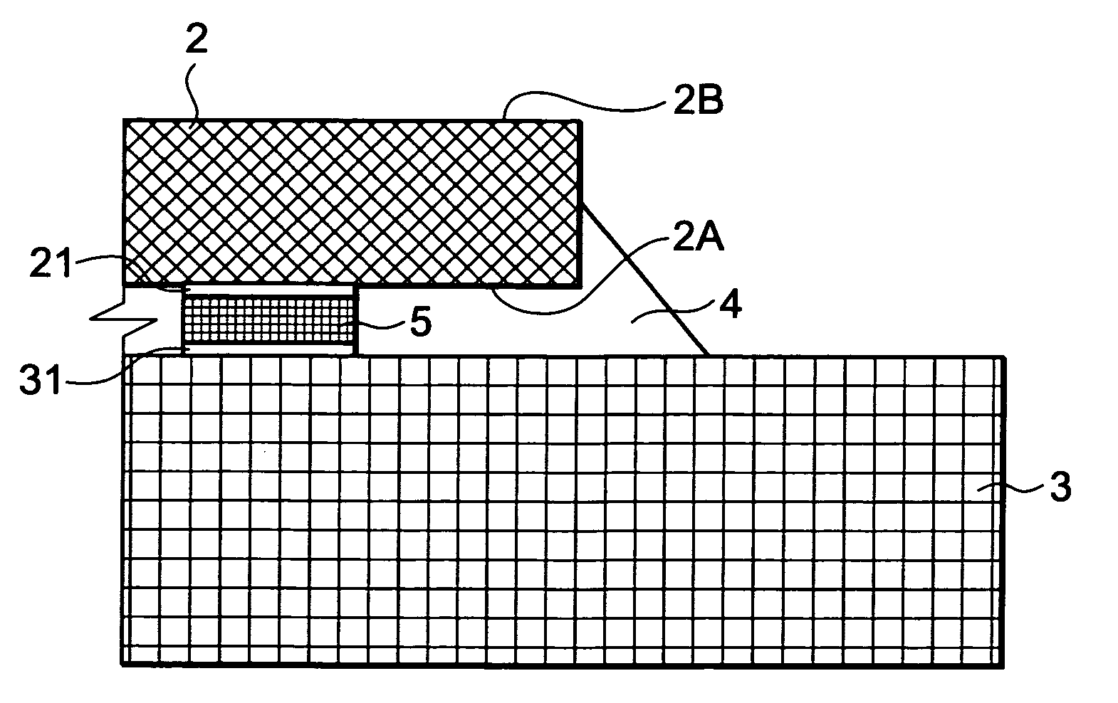
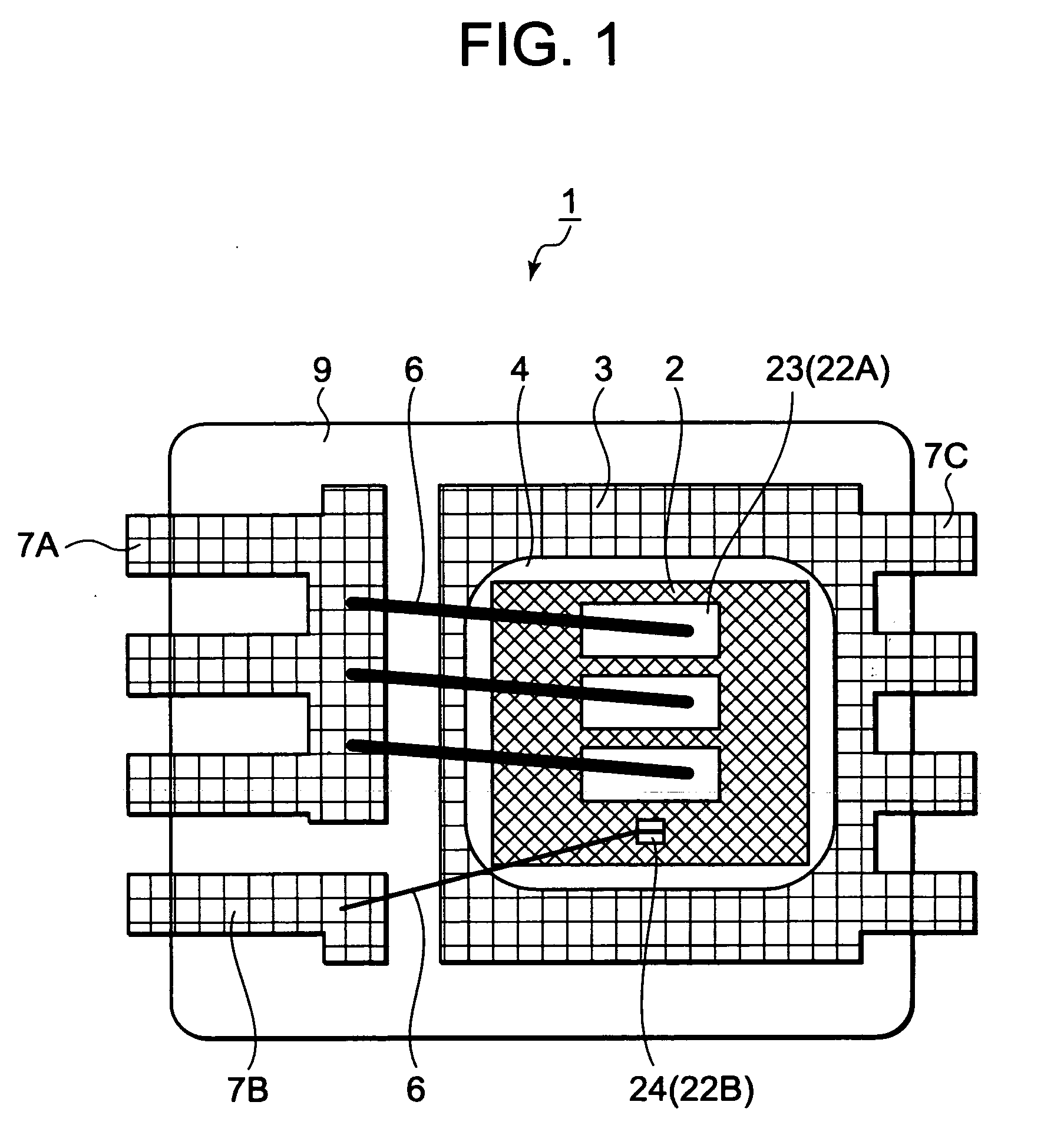
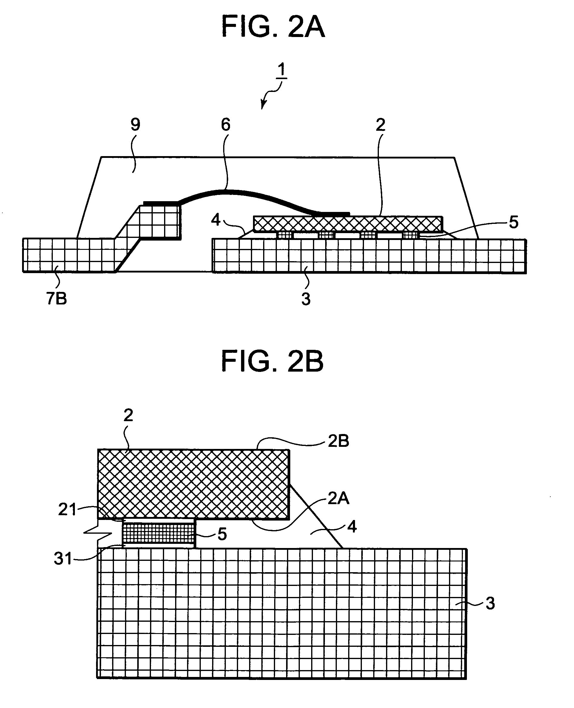
[0032]FIG. 1 illustrates a top view of a semiconductor device according to the exemplary embodiment 1 as seen through encapsulating resin; FIG. 2 illustrates a schematic side view of the semiconductor device according to the exemplary embodiment 1 as seen through the encapsulating resin; and FIG. 2B is a partially enlarged sectional view of FIG. 2A. The semiconductor device 1 is a transistor package and includes a semiconductor chip 2, die pad 3 being a first conductive frame, underfill resin 4 being a filler, lead-free solder 5, aluminum wire 6 being electrical connection means, source lead 7A being a second conductive frame, gate lead 7B being a second conductive frame, and encapsulating resin 9.

[0033]The semiconductor chip 2 is MOSFET, i.e., a transistor chip. The semiconductor chip 2 includes a first principal surface 2A having a region opposite the die pad 3 being the first conductive frame and a second principal surface 2B being a principal surface on the side opposite from th...

second exemplary embodiment

[0054]A semiconductor device fabricating method different from that of the exemplary embodiment 1 will be described below. In the following description, the same reference numerals are applied to parts corresponding to those of the exemplary embodiment 1, and an explanation thereof is appropriately omitted.

[0055]A semiconductor device according to the exemplary embodiment 2 is similar to that of the exemplary embodiment 1 in terms of the basic structure and fabrication method other than the following points. That is, a difference between the exemplary embodiment 1 and the exemplary embodiment 2 lies in that, according to the exemplary embodiment 1, the conductive pattern 21 on the surface of the first principal surface 2A is formed by etching the conductive pattern 21 by use of a resist mask, but according to the exemplary embodiment 2, the conductive pattern 21 is formed by a lift-off process. Another difference between exemplary embodiment 1 and the exemplary embodiment 2 lies in ...

third exemplary embodiment

[0062]An example of semiconductor device having a structure different from those of the exemplary embodiments 1 and 2 will be described below. The semiconductor device according to the exemplary embodiment 3 is similar to that of the exemplary embodiment 1 in terms of the basic structure and fabrication method other than the following points. That is, a difference between the exemplary embodiment 1 and the exemplary embodiment 3 lies in that, according to the exemplary embodiment 1, a column-shaped lead-free solder 5 is arranged within a circle drawn around a center C of the opposite region between the semiconductor chip 2 and the die pad 3 and having a diameter corresponding to a narrow side L of the opposite region, but according to the exemplary embodiment 3, a column-shaped lead-free solder 5 is arranged in a position in which the column-shaped lead-free solder 5 overlaps, in a plan view, a pad (source pad 22A) which is among pads formed on the second principal surface of the se...


PUM


Abstract

A semiconductor device includes a semiconductor chip having a current path between a first principal surface and a second principal surface opposite from the first principal surface, a first conductive frame having an opposite region to the first principal surface, and a second conductive frame electrically connected via electrical connection member to a pad formed on the second principal surface. In a gap between the first principal surface and the first conductive frame, there are arranged multiple column-shaped lead-free solders which are arranged within a circle drawn around a center of the opposite region and having a diameter corresponding to a narrow side of the opposite region, and which electrically connects the first conductive frame with the semiconductor chip, and a filler which is filled between the multiple column-shaped lead-free solders.

Description

INCORPORATION BY REFERENCE[0001]This application is based upon and claims the benefit of priority from Japanese Patent Application No. 2009-007793 which was filed on Jan. 16, 2009, the disclosure of which is incorporated herein in its entirety by reference.BACKGROUND OF THE INVENTION[0002]1. Field of the Invention[0003]The present invention relates to a semiconductor device and fabrication method thereof.[0004]2. Description of Related Art[0005]In mounting a semiconductor chip on a package substrate or lead frame, a method is typically used which connects a surface (rear surface) on the side opposite from a surface (front surface) of the semiconductor chip element with the package substrate or lead frame by use of a mounting material. On the other hand, for CPU (Central Processing Unit) and the like particularly requiring a multiple-pin structure, miniaturization and slim structure, a flip chip mounting method is also used in which the front surface of a semiconductor chip, facing a...

Claims


Application Information

Patent Timeline
IPC IPC(8): H01L23/488H01L21/56
CPCH01L21/563H01L23/3107H01L23/49513H01L23/49524H01L23/49562H01L24/02H01L24/06H01L24/11H01L24/12H01L24/16H01L24/17H01L24/40H01L24/45H01L24/49H01L24/73H01L24/81H01L24/92H01L2224/03H01L2224/0401H01L2224/04042H01L2224/05553H01L2224/0603H01L2224/1147H01L2224/13099H01L2224/45124H01L2224/48091H01L2224/48247H01L2224/48472H01L2224/4903H01L2224/49051H01L2224/49171H01L2224/73203H01L2224/73257H01L2224/73265H01L2224/81192H01L2224/81801H01L2924/01004H01L2924/01005H01L2924/01013H01L2924/01015H01L2924/01022H01L2924/01028H01L2924/01029H01L2924/0103H01L2924/01047H01L2924/0105H01L2924/01078H01L2924/01079H01L2924/01082H01L2924/01083H01L2924/014H01L2924/13091H01L24/48H01L2224/16245H01L2224/32245H01L2224/73204H01L2924/01006H01L2924/01033H01L24/29H01L2924/0132H01L2924/0133H01L2224/1131H01L2924/0134H01L2224/29111H01L2224/48699H01L2224/73221H01L2224/40247H01L2924/1306H01L2924/00014H01L2924/00H01L2924/01012H01L2924/01032H01L2924/01051H01L2924/3512H01L2924/351H01L2224/40095H01L2924/181H01L2224/40245H01L2224/84801H01L2224/83801H01L2224/8485H01L2224/84345H01L24/03H01L24/05H01L24/13H01L24/84H01L2924/00012H01L2224/37099
Inventor ANDOU, HIDEKO
Owner RENESAS ELECTRONICS CORP
Why Eureka
Try Eureka