Strain balanced light emitting devices

a light-emitting device and strain-balance technology, which is applied in the direction of semiconductor/solid-state device manufacturing, semiconductor devices, and electrical equipment, can solve the problems of not every injected electron and hole can recombine with each other, reduce iqe, and reduce iqe, so as to enhance the flexibility of proper device design and improve the performance of light-emitting devices

Inactive Publication Date: 2010-07-29
ZHEJIANG INVENLUX TECH
View PDF11 Cites 64 Cited by
  • Summary
  • Abstract
  • Description
  • Claims
  • Application Information

AI Technical Summary

Benefits of technology

[0008]The present invention improves light emitting device performance in various aspects. In some of the embodiments, before the growth of device active-region, a relaxation-enhancement-layer (REL) and a strain-balancing layer (SBL) are deposited in sequence for preparation of the active-region growth. A REL is used to help SBL to reach its strain-free status in an accelerated way, facilitating SBL to provide lattice template for the active-region achieving balanced-strain status. The strain-balancing layer is made of InxAlyGa1-x-yN (0≦x≦1, 0≦y≦1, x+y≦1), whose lattice-constant is tailo

Problems solved by technology

In practice, however, not every injected electron and hole can recombine with each other.
Beside these, improper active-region designs can also lead to reduced IQE.
Lattice mismatch will bring in strain, which can generate defects, resulting in IQE reduction.
Unfortunately, nitride semiconductors, especially In-containing nitrides, which are indispensable in realizing solid-s

Method used


Image

  • Strain balanced light emitting devices
  • Strain balanced light emitting devices
  • Strain balanced light emitting devices

Examples


Embodiment Construction

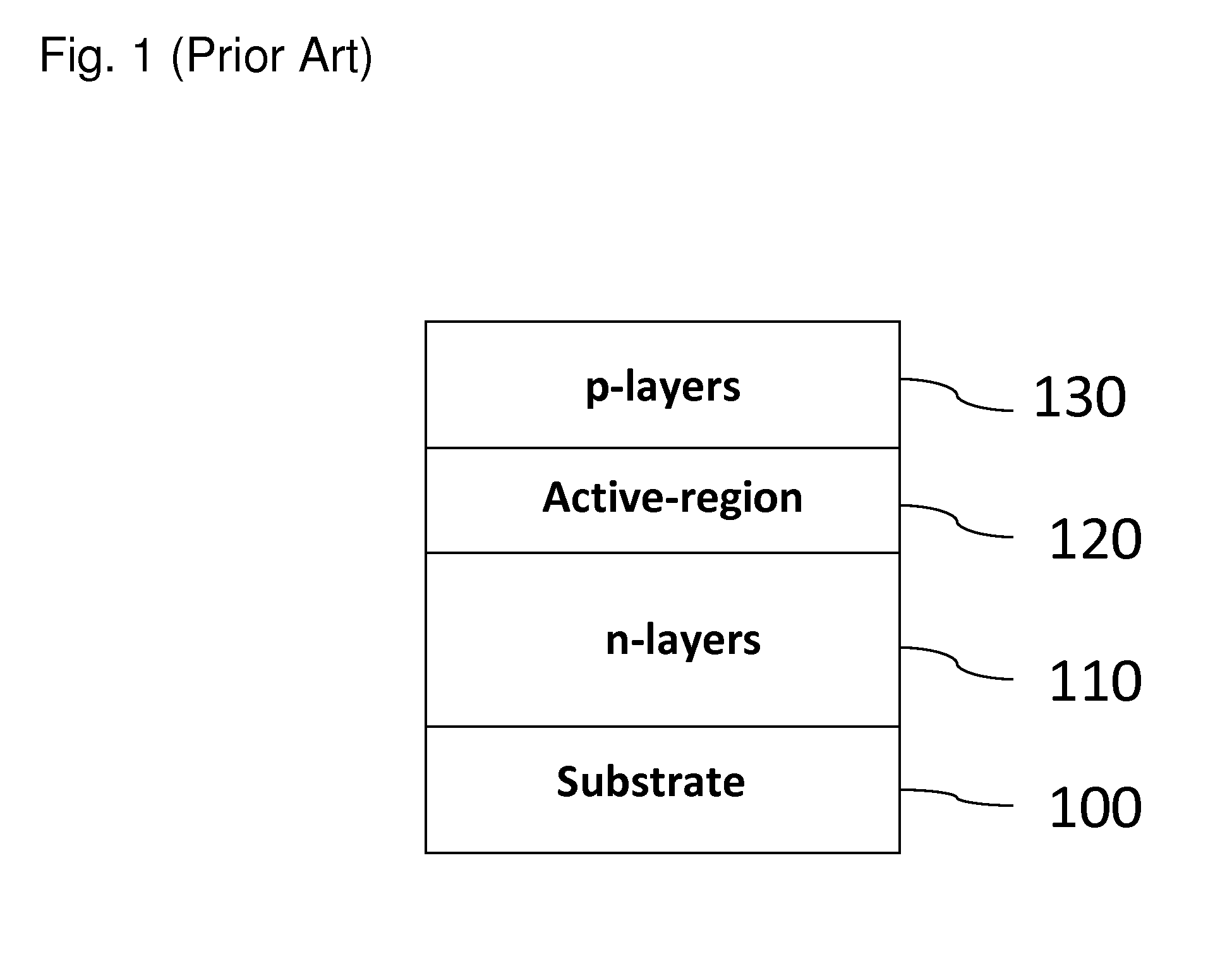
[0038]In the prior art light-emitting devices, the lattice-constant of the active-region is determined by the n-type base layers and there is no freedom to adjust the active-region lattice constant for a better performance. FIG. 1 shows a schematic cross-sectional structure of a prior art light-emitting device, consisting of a substrate 100, an electron-supplier n-type contact layer(s) 110, an active-region 120, and a hole-supplier p-type layer(s) 130.

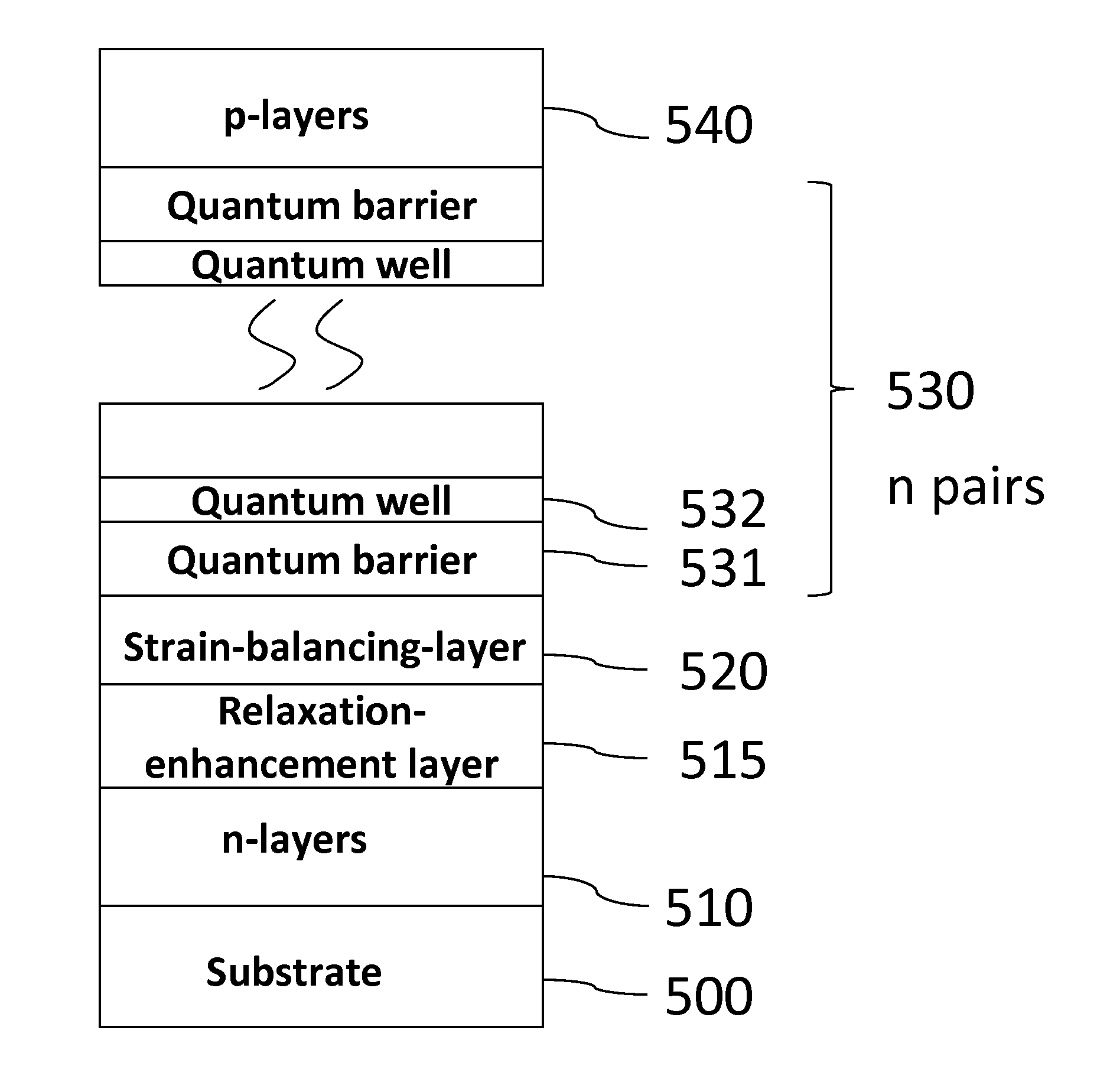
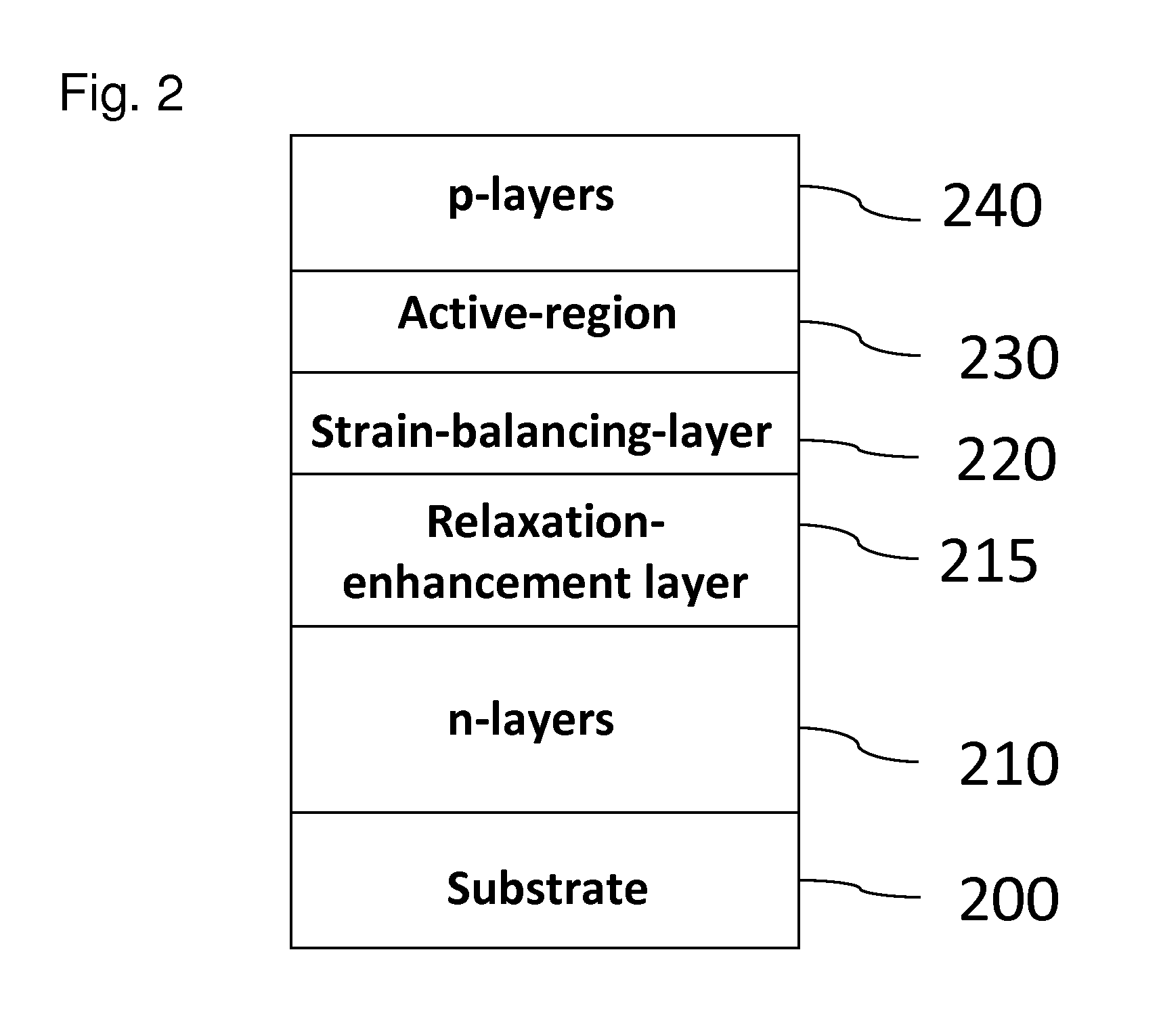
[0039]The present invention proposes a strain-balancing layer under the active-region in a light-emitting device for improved device performance. In the embodiments for LEDs, as schematically shown in FIG. 2, the strain-balanced structure includes a substrate 200, an electron injection layer (n-layer) 210, a relaxation-enhancement-layer 215, a strain-balancing layer 220, an active region 230, and a hole-injection layer (p-layer) 240. The strain-balancing layer 220 serves as lattice template to realize a strain-balanced active-region.

[0...


PUM


Abstract

A strain balanced active-region design is disclosed for optoelectronic devices such as light-emitting diodes (LEDs) and laser diodes (LDs) for better device performance. Lying below the active-region, a lattice-constant tailored strain-balancing layer provides lattice template for the active-region, enabling balanced strain within the active-region for the purposes of 1) growing thick, multiple-layer active-region with reduced defects, or 2) engineering polarization fields within the active-region for enhanced performance. The strain-balancing layer in general enlarges active-region design and growth windows. In some embodiments of the present invention, the strain-balancing layer is made of quaternary InxAlyGa1-x-yN (0≦x≦1, 0≦y≦1, x+y≦1), whose lattice-constant is tailored to exert opposite strains in adjoining layers within the active-region. A relaxation-enhancement layer can be provided beneath the strain-balancing layer for enhancing the relaxation of the strain-balancing layer.

Description

CROSS-REFERENCE TO RELATED APPLICATION[0001]This application claims priority benefit of provisional application No. 61 / 147,043 filed on Jan. 23, 2009, the content of which is hereby incorporated by reference in its entirety.FIELD OF INVENTION[0002]The present invention relates generally to semiconductor light-emitting devices and more particularly to improving the active-region performances of the light-emitting devices.BACKGROUND OF THE INVENTION[0003]In a semiconductor light-emitting device, negative-charge carriers and positive charge carriers, or, technically termed as electrons and holes, are driven (injected) from opposite contacts to meet in the light-emitting region, the so-called active-region. A photon is emitted if an injected electron and an injected hole annihilate with each other in the active-region. This process is called radiative recombination process. The figure-of-merit for the radiative recombination is called internal quantum efficiency (IQE), which equals to t...

Claims


Application Information

Patent Timeline
IPC IPC(8): H01L33/00H01L21/20
CPCH01L33/06H01L33/32H01L33/12Y10S438/938
Inventor YAN, CHUNHUI
Owner ZHEJIANG INVENLUX TECH
Why Eureka
Try Eureka