Electronic member, electronic part and manufacturing method therefor

a technology of electronic parts and electronic components, applied in the field of electronic components, can solve the problems of increasing the amount of organic substances to be added to the composition substance, voids are likely to remain, and bonding failures, and achieves high heat-resistance silver oxide, high heat-liberation, and reduced pitch spacing

Inactive Publication Date: 2010-08-05
HITACHI LTD
View PDF14 Cites 38 Cited by
  • Summary
  • Abstract
  • Description
  • Claims
  • Application Information

AI Technical Summary

Benefits of technology

[0022]The above-described technique makes it possible to provide an electronic part, including one or more connection terminals set up in a circuit board, and one or more electrode terminals set up in an electronic member, wherein the one or more electrode terminals are electrically bonded to the one or more connection terminals via a bonding layer, the bonding layer being mainly composed of sintered silver whose crystalline particle diameter is equal to 1000 nm or less, the entire surface or a partial surface of the electrode surface other than the bonding layer being a coarsely-grained layer of metallic silver.
[0023]The present invention employs the technique whereby the entire Ag-metalized layer or a partial Ag-metalized layer is oxidized into the silver-oxide layer. On account of this feature, a pitch spacing with which the Ag-metalized electrode can be formed becomes the pitch spacing with which the bonding is made implementable by the present invention. Namely, the electronic member becomes a one in which there scarcely occurs a decrease in the pitch spacing caused by the supply method for the bonding material. In this way, according to the present invention, it becomes possible to supply, with a microscopic pitch and in a thin manner, the bonding portion in which the high heat-liberation and high heat-resistant silver oxide is used. This feature allows the high-density implementation with a high accuracy.

Problems solved by technology

As a result of the experiments, it has been found out that the following problems exist.
There has occurred a problem, however, that the organic-substance amount to be added into the composition substance increases.
This problem has prevented the silver-oxide particles from being supplied in a closely-packed manner, thereby resulting in the occurrence of a bonding failure.
As a result, there exists a problem that, if a void exists before the bonding, this void is likely to remain as the void as it is after the bonding as well.
There has occurred a problem, however, that an aggregation among the silver-oxide particles appears unless the silver-oxide particles are coated with an organic substance after the synthesis.
As a result, there has occurred a problem that, when the silver-oxide particles are used as the bonding material, the temperature for eliminating the organic substance rises, and that the bonding temperature rises accordingly.
In this way, it has been found out that, in the printing of the pasted material, the supply of the pasted material with the microscopic pitch is difficult, and that the bonding with a high reliability is impossible.
After the bonding, this spread of the bonding material has resulted in the occurrence of a short-circuit between electrodes.

Method used


Image

  • Electronic member, electronic part and manufacturing method therefor
  • Electronic member, electronic part and manufacturing method therefor
  • Electronic member, electronic part and manufacturing method therefor

Examples


embodiment 1

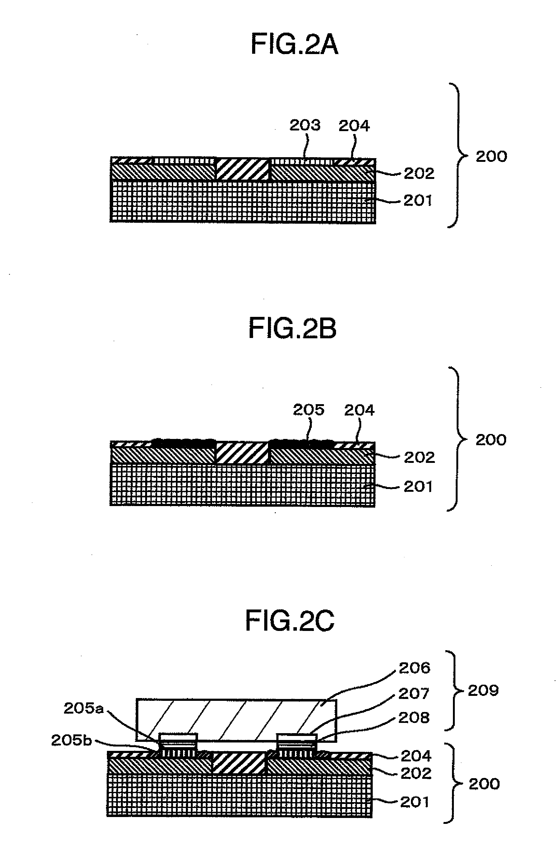
[0098]In the first embodiment, an Ag-metalized layer is formed onto a CU wiring on the circuit board, using the electrolytic plating method. The thickness of the Ag-metalized layer is equal to 5 μm.

[0099]Next, the Ag-metalized layer is oxidized into a silver-oxide layer, using the anode oxidization method. In the anode oxidization, a sodium-hydroxide (NaOH) aqueous solution is used, then maintaining the current density (mA / cm2) at a constant value. A Ni electrode is used as an opposed electrode.

[0100]Changing the mole concentration of the sodium-hydroxide aqueous solution and the current value changes the pH and the current density, respectively. Then, the relationship among the pH, the current density, and the thickness of the silver-oxide layer is checked and clarified. The thickness of the silver-oxide layer is determined by cutting out its sample cross-section, observing the cross-section using a scanning electron microscope, and averaging 50 points in an arbitrary field-of-view...

embodiment 2

[0102]A 5-μm-thick Ag-metalized layer is formed onto the CU wiring on the circuit board, using the electrolytic plating method. Then, the Ag-metalized layer is oxidized into a silver-oxide layer, using the ozone oxidization method. At this time, a 150-° C. and 5-vol %-ozone-concentration gas is sprayed over the Ag-metalized layer. It has been confirmed that this spray produces the silver-oxide layer, and that the thickness of the silver-oxide layer increases in accompaniment with an increase in the time during which the gas is sprayed.

embodiment 3

[0103]In the third embodiment, the cross-sections of the silver-oxide layers manufactured in the first and second embodiments are observed using the scanning electron microscope. As a result of the execution of the one-hundred-thousands-times-magnification observation, a-few-nm to a-few-tens-nm several voids are merely observed in a dispersed manner. Accordingly, it has been found out that the silver-oxide layers with almost no void are formed. It is conceivable that this result is attributed to the fact that, when the Ag-metalized layers are oxidized into the silver-oxide layers, its reaction becomes a one where an increase in the volume occurs.

[0104]As the comparison with the above-described cases, a pressured-powder material is manufactured by imparting a 100-MPa pressure application to 1-μm to 3-μm-particle-diameter silver-oxide particles. A resin is embedded into the pressured-powder material manufactured, and its cross-section is cut out, then observing the cross-section using...


PUM

PropertyMeasurementUnit
thicknessaaaaaaaaaa
curvature radiusaaaaaaaaaa
melting pointaaaaaaaaaa

Abstract

When silver oxide is reduced to silver, a large number of cores of metallic silver are formed inside the silver oxide. Then, the silver oxide is reduced in a manner of being hollowed out while its original outer configuration is being maintained. As a result, the curvature of the silver generated becomes larger. The utilization of this microscopic-particle implementation mechanism allows accomplishment of the bonding even if the silver oxide is supplied not in a particle-like configuration, but in a closely-packed layer-like configuration. In the present invention, there is provided an electronic member including an electrode for inputting/outputting an electrical signal, or a connection terminal for establishing a connection with the electrical signal, wherein the uppermost surface of the electrode or the connection terminal is a silver-oxide layer.

Description

BACKGROUND OF THE INVENTION[0001]The present invention relates to electronic members designed on a premise that mutual electrical bonding of the electronic members (e.g., bonding of a semiconductor element and a circuit member) is performed. More particularly, it relates to an electronic part constituted by implementing the electronic members, and its implementation method. Hereinafter, such components as semiconductor elements and circuit members will be generically referred to as “electronic members”.[0002]In recent years, there has been a significant increase in the request for the multi-function implementation, high-speed implementation, and light-thin-&-short-small implementation of electronic appliances which start with mobile appliances. What has become important in order to satisfy this request is the narrow-pitch implementation and low-back implementation of the electrode of an electronic appliance for inputting / outputting an electrical signal concerned.[0003]Meanwhile, as ...

Claims


Application Information

Patent Timeline
Patent Type & Authority Applications(United States)
IPC IPC(8): H05K7/00H01B1/08H01B1/02H01B1/12H05K1/02H05K1/09B05D5/12C25D11/34
CPCC25D11/34H01L23/481H01L23/49582H01L23/49811H01L23/49833H01L23/49866H01L23/50H01L24/13H01L24/16H01L24/27H01L24/32H01L24/45H01L24/50H01L24/81H01L24/83H01L25/0657H01L25/50H01L33/62H01L2224/13025H01L2224/13099H01L2224/13109H01L2224/16145H01L2224/16225H01L2224/29339H01L2224/32225H01L2224/32245H01L2224/45144H01L2224/48091H01L2224/48105H01L2224/48177H01L2224/48227H01L2224/48247H01L2224/73204H01L2224/73265H01L2224/81193H01L2224/81201H01L2224/83801H01L2224/8384H01L2224/85205H01L2225/06513H01L2225/06541H01L2924/01004H01L2924/01011H01L2924/01013H01L2924/01014H01L2924/01016H01L2924/01022H01L2924/01029H01L2924/0103H01L2924/01046H01L2924/01047H01L2924/0105H01L2924/01078H01L2924/01079H01L2924/01082H01L2924/01327H01L2924/10253H01L2924/12044H01L2924/19041H01L2924/19042H01L2924/19043H01L2924/19105H05K1/185H05K3/244H05K3/32H05K2201/10636H05K2201/10674H05K2203/0315H05K2203/1157H05K2203/121H01L24/48H01L2224/2919H01L2924/01005H01L2924/01006H01L2924/01019H01L2924/01033H01L2924/01042H01L2924/014H01L2924/0665H01L2924/0132H01L2924/0133H01L2924/15747H01L2924/1576H01L2224/29139H01L2224/81395H01L2224/29111H01L2924/01028H01L2924/12041H01L2224/81009H01L2224/8184H01L2224/81486H01L2924/00014H01L2924/00H01L2924/00012H01L2924/3512H01L2924/053H01L2924/351H01L2924/00011H01L24/73H01L23/3142H01L2224/05009H01L2224/05568H01L2224/05001H01L2224/05124H01L2224/05139H01L2224/05144H01L2224/05147H01L2224/05155H01L2224/05166H01L2224/05169H01L2224/05639H01L2924/181H01L24/86H01L24/05H01L24/03H01L2224/0401Y02P70/50H01L2224/83205
Inventor IDE, EIICHIMORITA, TOSHIAKIYASUDA, YUSUKE
Owner HITACHI LTD
Why Eureka
Try Eureka