Graphene grown substrate and electronic/photonic integrated circuits using same

a technology of graphene and substrate, which is applied in the direction of crystal growth process, crystal growth process, polycrystalline material growth, etc., can solve the problems of inconvenient industrial application, method has a manufacturing cost problem, and the type of substrate that can be used is limited, so as to achieve low cost

Inactive Publication Date: 2010-08-12
HITACHI LTD
View PDF2 Cites 98 Cited by
  • Summary
  • Abstract
  • Description
  • Claims
  • Application Information

AI Technical Summary

Problems solved by technology

The above methods have the following problems: The method reported by Novoselov et al. is feasible on an experimental basis, but is not suitable for industrial applications because it is difficult for the method to provide large size substrates.
However, the method has a manufacturing cost problem because it requires a specially designed ultrahigh vacuum apparatus.
However, the method requires high temperature treatment (about 1350° C.) in ultrahigh vacuum, and therefore the type of substrate that can be used is limited and also the manufacturing cost is high.

Method used


Image

  • Graphene grown substrate and electronic/photonic integrated circuits using same
  • Graphene grown substrate and electronic/photonic integrated circuits using same
  • Graphene grown substrate and electronic/photonic integrated circuits using same

Examples


first embodiment

of Present Invention

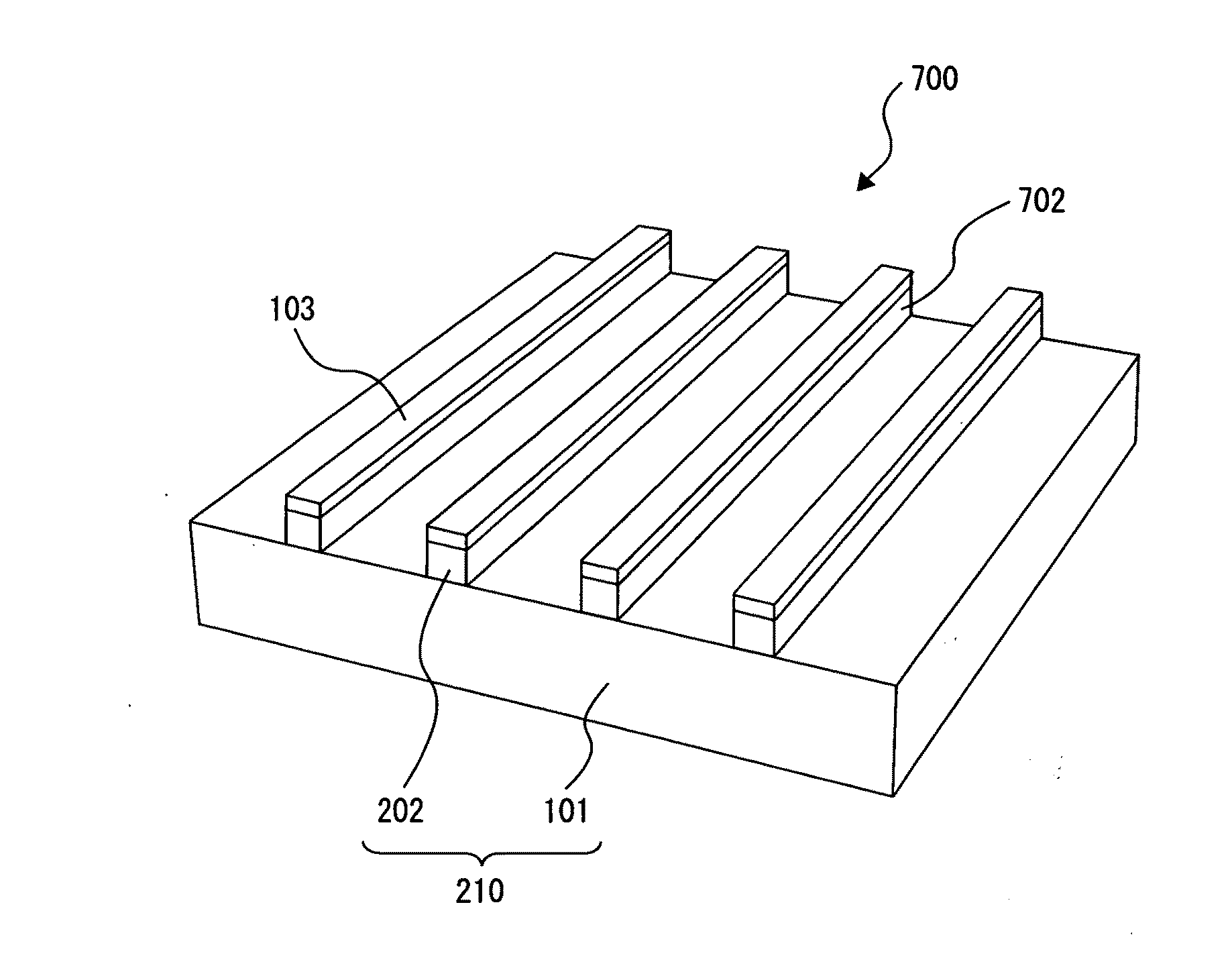
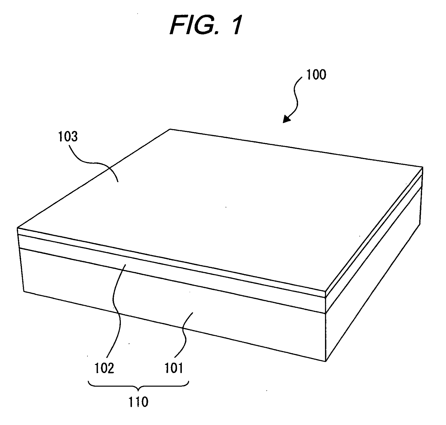
[0057]FIG. 1 is a schematic illustration showing a perspective view of an exemplary substrate having a graphene layer grown thereon according to a first embodiment of the present invention. First, an aluminum oxide (α-alumina, Al2O3) film 102 is formed on a single crystalline silicon substrate 101 by sputtering or the like. Thus, a substrate 110 having atomic layers of metal oxide on its surface is obtained. The aluminum oxide film 102 preferably has an average thickness of 10 nm or more and 500 nm or less. An average thickness less than 10 nm is undesirable for the following reason: The crystal grains of the polycrystalline aluminum oxide film 102 do not coalesce sufficiently at thicknesses less than 10 nm (for example, the aluminum oxide film 102 grows like islands). Thus, the surface coverage of the silicon substrate 101 with the aluminum oxide film 102 is insufficient, resulting in poor surface smoothness of the aluminum oxide film 102. On the other hand, an ...

second embodiment

of Present Invention

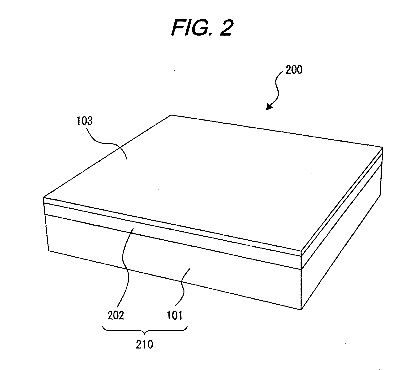
[0064]FIG. 2 is a schematic illustration showing a perspective view of an exemplary substrate having a graphene layer grown thereon according to a second embodiment of the present invention. First, a silicon oxide (SiO2) film 202 is formed on a single crystalline silicon substrate 101 by thermal oxidation or the like. Thus, a substrate 210 having atomic layers of metal oxide on its surface is obtained. The silicon oxide film 202 preferably has an average thickness of 10 to 500 nm. An average thickness of the polycrystalline silicon oxide film 202 less than 10 nm is undesirable because of local nonuniformity in the film thickness (i.e., poor surface smoothness). One reason for such thickness nonuniformity is the fact that island growth occurs during the initial growth stage of the silicon oxide film 202. On the other hand, an average thickness more than 500 nm is also undesirable because the resulting silicon oxide film 202 is prone to suffer from cracks caused by...

third embodiment

of Present Invention

[0067]FIG. 3 is a schematic illustration showing a perspective view of an exemplary substrate having a graphene layer grown thereon according to a third embodiment of the present invention. First, a mullite (3Al2O3.2SiO2) film 302 is formed on a single crystalline silicon substrate 101 by sputtering or the like. Thus, a substrate 310 having atomic layers of metal oxide on its surface is obtained. The mullite film 302 preferably has an average thickness of 10 to 500 nm. An average thickness less than 10 nm is undesirable because the grains of the polycrystalline mullite film 302 do not coalesce sufficiently resulting in poor surface coverage of the silicon substrate 101 with the mullite film 302. On the other hand, an average thickness more than 500 nm is also undesirable because the resulting mullite film 302 is prone to suffer from cracks caused by, e.g., thermal stresses undergone during subsequent processing, thus resulting in poor surface smoothness (as defin...


PUM

PropertyMeasurementUnit
surface roughnessaaaaaaaaaa
surface height Rzaaaaaaaaaa
grain sizeaaaaaaaaaa

Abstract

A graphene-on-oxide substrate according to the present invention includes: a substrate having a metal oxide layer formed on its surface; and, formed on the metal oxide layer, a graphene layer including at least one atomic layer of the graphene. The graphene layer is grown generally parallel to the surface of the metal oxide layer, and the inter-atomic-layer distance between the graphene atomic layer adjacent to the surface of the metal oxide layer and the surface atomic layer of the metal oxide layer is 0.34 nm or less. Preferably, the arithmetic mean surface roughness Ra of the metal oxide layer is 1 nm or less.

Description

CLAIM OF PRIORITY[0001]The present application claims priority from Japanese patent application serial no. 2009-242092 filed on Oct. 21, 2009, which further claims priority from Japanese patent application serial no. 2008-300556 filed on Nov. 26, 2008, the contents of which are hereby incorporated by reference into this application.BACKGROUND OF THE INVENTION[0002]1. Field of the Invention[0003]The present invention relates to graphenes for use in electronic and optical device applications. The invention particularly relates to substrates having a graphene layer grown thereon, and electro-optical integrated circuits formed in such a substrate.[0004]2. Description of Related Art[0005]Graphenes (also called graphene sheets) are a sheet of six-membered rings which does not form a closed surface, and are formed by connecting numerous benzene rings two-dimensionally. Carbon nanotubes are formed by rolling up a graphene sheet into a tubular structure. Graphites are formed by stacking mult...

Claims


Application Information

Patent Timeline
Patent Type & Authority Applications(United States)
IPC IPC(8): H01L29/12H01L31/0256H01L33/02
CPCC23C16/26C23C16/56C30B25/02C30B29/02H01L21/02381H01L29/78684H01L21/02488H01L21/02527H01L21/0262H01L29/78603H01L21/0242
Inventor OKAI, MAKOTOHIROOKA, MOTOYUKIKYOTANI, TAKASHIORIKASA, HIRONORI
Owner HITACHI LTD
Why Eureka
Try Eureka