Transparent electromagnetic wave shield member and method for manufacturing the same

a technology of electromagnetic wave shielding and electromagnetic wave, which is applied in the field of transparent electromagnetic wave shielding members, can solve the problems of generating moirè phenomenon, affecting the quality of photolithography, so as to achieve excellent electromagnetic wave shielding properties, prevent image degradation, and provide sufficient total light transmittance

Inactive Publication Date: 2010-08-19
TORAY IND INC
View PDF0 Cites 23 Cited by
  • Summary
  • Abstract
  • Description
  • Claims
  • Application Information

AI Technical Summary

Benefits of technology

[0015]By the present invention, it is possible to obtain a transparent electromagnetic wave shield member, which is free from a moirè phenomenon, and in which an excellent electromagnetic wave shielding properties and a sufficient total light transmittance based on an appropriate network structure are compatible. And, by the preferable embodiments of the present invention, a transparent electromagnetic wave shield member of which image degradation is more prevented can be obtained.
[0016]FIG. 1 An example of schematic cross sectional view of a transparent electromagnetic wave shield member of the present invention.
[0017]FIG. 2 An example of schematic cross sectional view of a transparent electromagnetic wave shield member of the present invention.
[0018]FIG. 3 An example of schematic cross sectional view of a transparent electromagnetic wave shield member of the present invention.
[0019]FIG. 4 A schematic cross sectional view which explains the manufacturing process of a transparent electromagnetic wave shield member of the present invention.

Problems solved by technology

However, in the photolithography method in which the transparent electromagnetic wave shield sheet is manufactured by using an electroconductive metal layer laminated on a transparent substrate, a lattice-like electroconductive metal layer (copper foil layer) of the substrate has a network structure of a large regular spacing, and in addition, since there is a thickening in intersection portion of the network, there is a problem that a moirè phenomenon is generated.
And, in cases where a regular pattern such as of lattice-like is provided to the electromagnetic wave shield substrate, there is a problem that, as the line width of this lattice becomes broader, this moirè phenomenon may generate more easily.
Furthermore, the process of photolithography is complicated and long, i.e., it is not a satisfactory method for the commercial needs of cost reduction.
Whereas, in order to make the electromagnetic wave shielding properties and visibility of the display picture compatible, a method is proposed that a black color resist layer is laminated on the patterned electroconductive metal layer, and said black color resist is left without peeling off (Patent reference 4), but after all, this also depends on a photolithography method, its process is complicated and long, i.e., it could not be said to be a satisfactory method for the commercial needs of cost reduction.
However, in these printing methods, it was difficult to print a high precision line width, and it was difficult to form a fine line pattern of 20 μm or less which is preferable for non-visibility of network pattern, and a moirè phenomenon was likely to generate on the display picture.
And, there remained a problem to be solved in the obtained electromagnetic wave shield member in view point of transparency.
However, since the electromagnetic wave shield member manufactured by this method has a thick line diameter of the electroconductive fiber, in cases where a sufficient shielding performance was demanded, there was a defect that an opening ratio decreases and visibility of picture decreases.
In this method, since the catalyst layer for the electroless plating is prepared by printing, it was difficult to narrow line width of the network and the line width of the network obtained after the plating was wide as 25 to 30 μm, and it was difficult to achieve an opening ratio for obtaining sufficient visibility.
Furthermore, a method is proposed in which a network pattern is drawn by coating silver salt which is a photosensitive material on a film and subjected to an exposure by ultraviolet ray through a mask pattern, to prepare a network pattern on a transparent support (Patent reference 7), but it has a defect that the process is complicated.
And, it is difficult to obtain a sufficient shielding performance by the prepared silver salt network only, and since it is necessary, after the network pattern is prepared, to thicken the electroconductive layer by plating, it has a defect that the process becomes more complicated.

Method used


Image

  • Transparent electromagnetic wave shield member and method for manufacturing the same
  • Transparent electromagnetic wave shield member and method for manufacturing the same
  • Transparent electromagnetic wave shield member and method for manufacturing the same

Examples


example 1

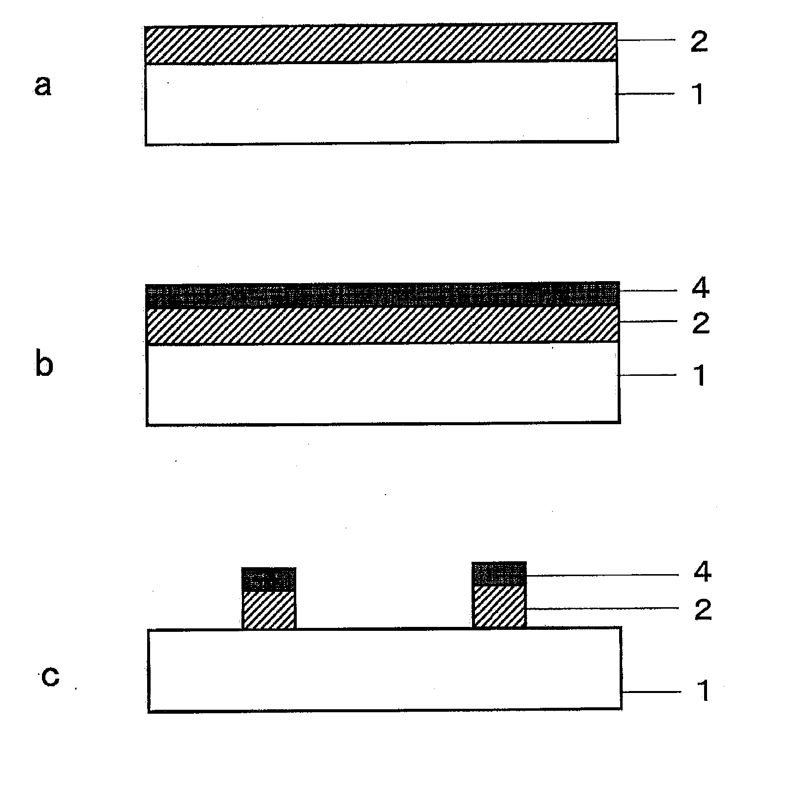
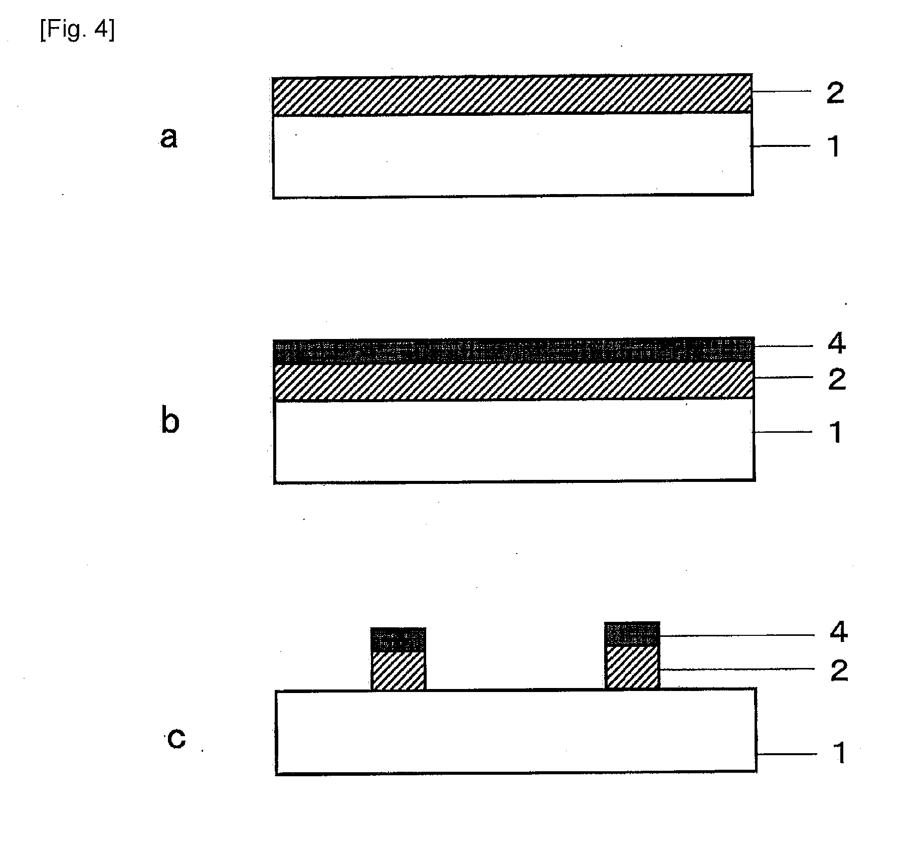
[0084]By sputtering copper (degree of vacuum: 0.5 Pa, target: copper, introduced gas ratio: Argon 100%) on one surface of a PET film (Lumirror (trademark) U34 produced by Toray Industries, Inc.) of a thickness 100 μm, a film was prepared in which a copper layer of a thickness 0.08 μm was formed on the PET.

[0085]Next, by sputtering method (degree of vacuum: 0.5 Pa, target: copper, introduced gas ratio: oxygen 100%), copper oxide of a thickness 0.05 μm was formed on the copper (the first metal oxide layer).

[0086]By irradiating the third harmonic of YAG laser of wavelength 355 nm to the opposite side to the transparent substrate (sputtering surface) of the film, a transparent electromagnetic wave shield member was prepared in which a network structure having a line width of 5 μm and a network structure spacing of 75 μm, based on a structure in which only a copper layer in square portion of one side 70 μm was abraded, was formed on the surface.

[0087]As shown in Table 1, the visibility, ...

example 2

[0088]After carrying out a vacuum vapor deposition (degree of vacuum: 3×10⁻³ Pa) of copper of only a thickness of 0.3 μm on the same PET film as that of Example 1, by further sputtering copper oxide of only a thickness 0.03 μm, a film in which a metal layer of a thickness 0.33 μm is formed on the PET was prepared.

[0089]By irradiating the third harmonic of YAG laser of wavelength 355 nm to the opposite side to the transparent substrate (the metal layer formed surface) of the prepared film, a transparent electromagnetic wave shield member was prepared in which a network structure having a line width of 5 μm and a network structure spacing of 75 μm, based on a structure in which only a copper layer in square portion of one side 70 μm was abraded, was formed on the surface.

[0090]As shown in Table 1, the visibility, electromagnetic wave shielding properties and moirè were all good.

example 3

[0091]In the same way as Example 2, after carrying out a vacuum vapor deposition of copper of only a thickness of 0.5 μm on the PET film, by further sputtering copper oxide of only a thickness 0.03 μm, a film in which a metal layer of a thickness 0.53 μm is formed on the PET, was prepared.

[0092]By irradiating the third harmonic of YAG laser of wavelength 355 nm to the opposite side to the transparent substrate (the metal layer formed surface) of the prepared film, a transparent electromagnetic wave shield member was prepared in which a network structure having a line width of 8 μm and a network structure spacing of 150 μm, based on a structure in which only a copper layer in square portion of one side 142 μm was abraded, was formed on the surface.

[0093]As shown in Table 1, the visibility, electromagnetic wave shielding properties and moirè were all good.


PUM

PropertyMeasurementUnit
thicknessaaaaaaaaaa
thicknessaaaaaaaaaa
thicknessaaaaaaaaaa

Abstract

The present invention aims to provide a transparent electromagnetic wave shield member, which is free from a moirè phenomenon which could not be solved by the prior art, and in which an excellent electromagnetic wave shielding properties and a sufficient total light transmittance based on an appropriate network structure are compatible, and a method for manufacturing the same.
The transparent electromagnetic wave shield member of the present invention is a transparent electromagnetic wave shield member in which a metal layer of an electroconductive metal network structure having a geometrical shape is formed on a transparent substrate, and which is characterized in that a spacing of said network structure is 200 μm or less, an opening ratio of the network structure is 84% or more, and in addition, a thickness of the electroconductive metal layer is 2 μm or less.
Furthermore, the method for manufacturing such transparent electromagnetic wave shield member is a method for manufacturing a transparent electromagnetic wave shield member in which a metal layer of a network structure having a geometrical shape is formed on a transparent substrate, which is characterized in that a metal layer of a thickness of 2 μm or less is provided on a transparent substrate and the metal layer is removed by laser abrasion to form a metal layer of a network structure having a spacing of the network structure of 200 μm or less, and in addition, an opening ratio of the network structure of 84% or more.

Description

TECHNICAL FIELD[0001]The present invention relates to a transparent electromagnetic wave shield member capable of fluoroscopy, which is used for image displaying parts such as plasma display panel (PDP) or cathode ray tube (CRT) which are electric products generating electromagnetic wave, and a method for manufacturing the same, and in addition, a filter and a display using the same.BACKGROUND ART[0002]In recent years, regulations relating to electromagnetic wave generated from electric products have been strengthened because of its radio frequency interference to various precision instruments, measuring instruments and digital instruments or influence to human body. For that reason, discharge of the electromagnetic wave is regulated by law, for example, there is a regulation by VCCI (Voluntary Control Council for Interference by data processing equipment electronic office machine). Therefore, in PDP which discharges especially a strong electromagnetic wave to outside the device fro...

Claims


Application Information

Patent Timeline
Patent Type & Authority Applications(United States)
IPC IPC(8): H05K9/00B05D5/12C23C14/14C23C14/34B23K26/00
CPCH01J11/10H05K9/0096H01J2211/446H01J11/44H05K9/00
Inventor MATSUI, YOSHITAKAKOTOURA, MASAAKIWATANABE, OSAMUYOSHIOKA, TADASHISAKAMOTO, KEITARO
Owner TORAY IND INC
Why Eureka
Try Eureka