Light-emitting diode light source module

a light source module and light-emitting diode technology, applied in the direction of basic electric elements, electrical equipment, semiconductor devices, etc., can solve the problems of reducing the reliability reducing the luminous efficiency of the light-emitting diode chip, and poor conversion efficiency, so as to increase the heat conduction substrate

Inactive Publication Date: 2010-08-19
CHI MEI LIGHTING TECH
View PDF0 Cites 44 Cited by
  • Summary
  • Abstract
  • Description
  • Claims
  • Application Information

AI Technical Summary

Benefits of technology

[0009]Therefore, one objective of the present invention is to provide a light-emitting diode light source module, in which light-emitting diode chips are embedded in a heat conduction substrate, so that the contact area between the light-emitting diode chips and the heat conduction substrate is increased. In addition, the volume of the heat conduction substrate is much larger than those of the light-emitting diode chips, and it is not necessary to use the conventional sliver glue to fix the light-emitting diode chips. Therefore, the heat produced by the light-emitting diode chips can be rapidly conducted to the external environment, and the issue of the reduction of the luminous flux per watt resulting from the superheat of the light-emitting diode chips can be effectively solved.
[0010]Another objective of the present invention is to provide a light-emitting diode light source module. In the manufacturing of the light-emitting diode light source module, light-emitting diode chips are directly integrated to a heat conduction substrate, and the semiconductor fabrication techniques including a film disposition technique, a photolithograph technique and an etching technique cooperating with the conventional wire bonding technique can be used to connect the light-emitting diode chips and the circuit on the circuit substrate. Therefore, it is unnecessary to use polyphthalamide to form a package base of the light-emitting diode, the formation of the conventional lead is not needed, and the process of combining the package base and the lead frame is not needed. Accordingly, in comparison with the conventional technique, the present invention has advantages of process simplification and low cost.
[0011]Still another objective of the present invention is to provide a light-emitting diode light source module. In the fabrication of the light-emitting diode light source module, an encapsulation material is filled between a transparent substrate and a heat conduction substrate by a batch method. In addition, a fluorescent layer may be entirely coated on the transparent substrate by a spin coating method or partially coated on the transparent substrate by a screen-printing method. Therefore, in comparison with the conventional package method of the light-emitting diode, it is unnecessary to pack the light-emitting diode chips one by one in the present invention. Accordingly, the thicknesses of the entire fluorescent layer and the entire encapsulation layer can be controlled, thereby increasing the uniformity of the process, effectively simplifying the package process and greatly reducing the package time.
[0012]Further another objective of the present invention is to provide a light-emitting diode light source module, in which a transparent substrate can be set with an optical structure, so that in addition to protecting the underlying light-emitting diode chips, the transparent substrate can enhance optical effects, such as increasing the light-extracting efficiency, enhancing the light uniformity and reducing the light-mixing distance, by designing the optical structure of the transparent substrate. Furthermore, a reflective layer may be disposed on a light-extracting side of the light-emitting diode chip, so that the light-extracting efficiency can be effectively increased.
[0013]Still further another objective of the present invention is to provide a light-emitting diode light source module, in which the conventional lead frame is not needed to connect a light-emitting diode package structure, so that the poor collinearity of the light-emitting diode chips caused by the non-uniform solders in the reflow process of the lead frame can be prevented.

Problems solved by technology

However, the conventional light-emitting diode chip generally cannot transform all of the input electric energy into light energy, and the electric energy is mostly lost in the form of thermal energy, so that the transform efficiency is poor.
If the heat cannot be effectively dissipated, the junction temperature of the light-emitting diode chip is further increased, thereby reducing the luminous efficiency of the light-emitting diode chip and decreasing the reliability of the light-emitting diode chip.
In addition, the metal heat sink 112 needs to be formed simultaneously with the lead frame 106, so that the irregular and large thickness difference of the lead frame 106 will further complicate the process to fabricate the lead frame 106 and causes a material waste issue.
These package and manufacture procedures all increase the complexity of the process of the light-emitting diode illuminant module 100.
Furthermore, the light-emitting diode chip 102 is usually connected to the metal heat sink 112 by sliver glue, so that the heat conduction of the light-emitting diode chip 102 is limited by the heat-conducting ability of the silver glue, thereby resulting in a poor heat-dissipating effect.
When the circuit board 134 is a metal core printed circuit board, the cost of such circuit board 134 is high because the process of the metal core printed circuit board is complicated.

Method used


Image

  • Light-emitting diode light source module
  • Light-emitting diode light source module
  • Light-emitting diode light source module

Examples


Embodiment Construction

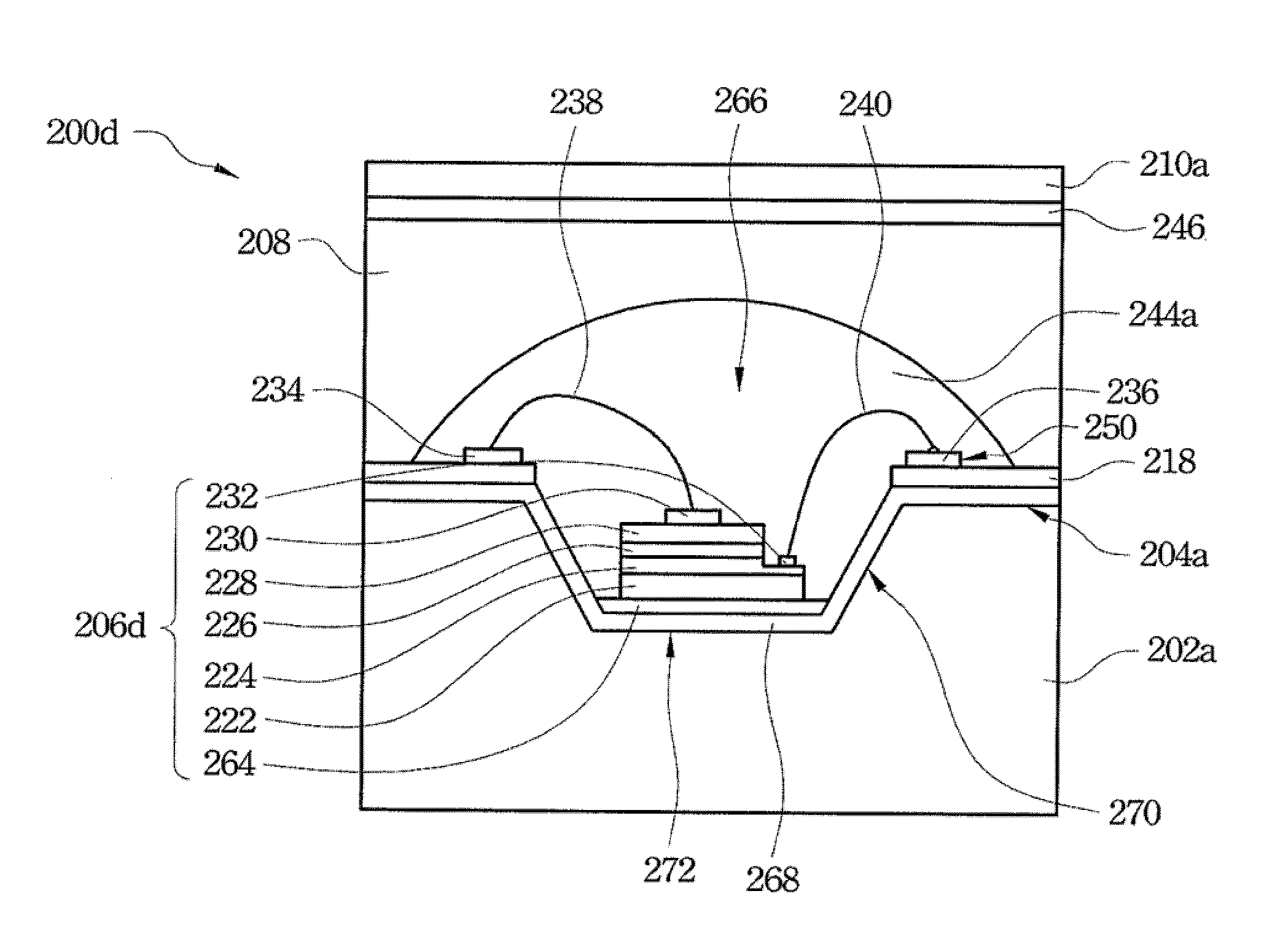
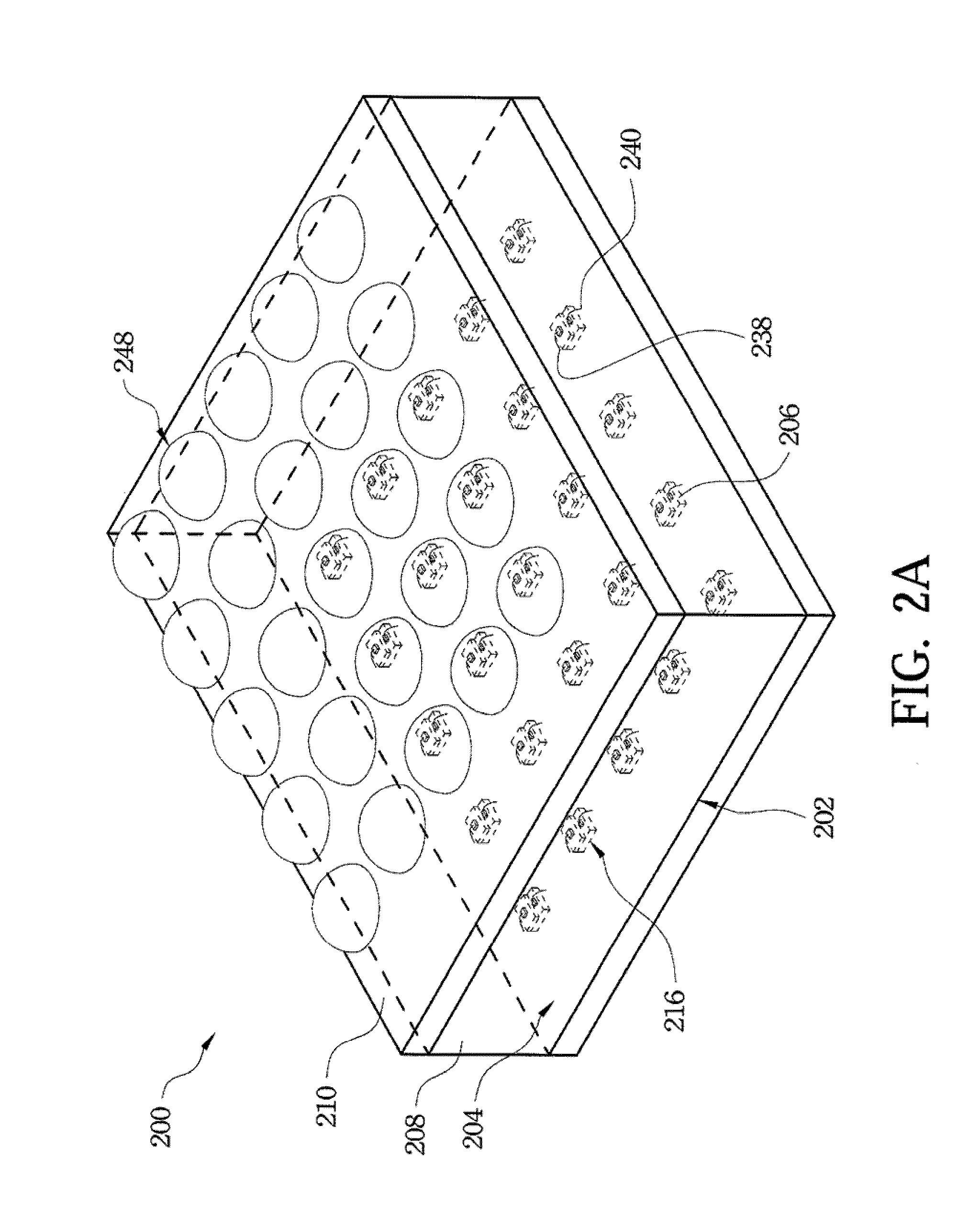
[0027]Refer to FIGS. 2A and 2B. FIGS. 2A and 2B respectively illustrate a three-dimensional perspective drawing and a cross-sectional view of a light-emitting diode light source module in accordance with a preferred embodiment of the present invention. In one exemplary embodiment, a light-emitting diode light source module 200 comprises a heat conduction substrate 202, a plurality of light-emitting diode chips 206, one or more insulation layers 218, one or more electric conduction layers 250, an encapsulation layer 208 and preferable a transparent substrate 210. The light-emitting diode chips 206 can be arranged according to the practical requirements, so that the light-emitting diode chips 206 can be arranged uniformly or irregularly.

[0028]In one embodiment, each of the light-emitting diode chips 206 is a light-emitting diode structure with horizontal electrodes. Each of the light-emitting diode chips 206 mainly comprises a substrate 222, a first conductivity type semiconductor lay...


PUM


Abstract

A light-emitting diode (LED) light source module is described, comprising: a heat conduction substrate, wherein a surface of the heat conduction substrate includes a plurality of recesses; a plurality of light-emitting diode chips respectively disposed in the recesses; an insulation layer disposed on the surface of the heat conduction substrate outside of the recesses; an electric conduction layer disposed on the insulation layer, wherein the light-emitting diode chips are electrically connected to the electric conduction layer; and an encapsulation layer covering the light-emitting diode chips, the electric conduction layer and the insulation layer.

Description

RELATED APPLICATIONS[0001]This application claims priority to Taiwan Application Serial Number 98105158, filed Feb. 18, 2009, which is herein incorporated by reference.FIELD OF THE INVENTION[0002]The present invention relates to a light source module, and more particularly to a light-emitting diode (LED) light source module.BACKGROUND OF THE INVENTION[0003]With the trend towards energy conservation and environmental protection, illuminant modules using light-emitting diodes as light sources have gradually replaced common incandescent lamps and fluorescent tubes. Currently, the light-emitting diode illuminant module is fabricated by soldering surface mounting device (SMD) light-emitting diode package structures onto a circuit board using a surface mount technique. The power is provided to the circuit board and is delivered respectively to p-type electrodes and n-type electrodes of light-emitting diode chips through lead frames of the light-emitting diode package structure to make the...

Claims


Application Information

Patent Timeline
Patent Type & Authority Applications(United States)
IPC IPC(8): H01L33/00
CPCH01L25/0753H01L33/005H01L33/507H01L33/54H01L33/58H01L33/62H01L33/642H01L2924/01322H01L2224/48247H01L2224/48091H01L2924/00014H01L2924/00
Inventor CHEN, SHI-MINGLI, WEN-LIANGCHU, CHANG-HSINWANG, HSING-MAO
Owner CHI MEI LIGHTING TECH
Why Eureka
Try Eureka