Non-volatile semiconductor storage device and method of manufacturing the same
- Summary
- Abstract
- Description
- Claims
- Application Information
AI Technical Summary
Benefits of technology
Problems solved by technology
Method used
Image

Examples
first embodiment
Configuration of Non-Volatile Semiconductor Storage Device 100 in First Embodiment
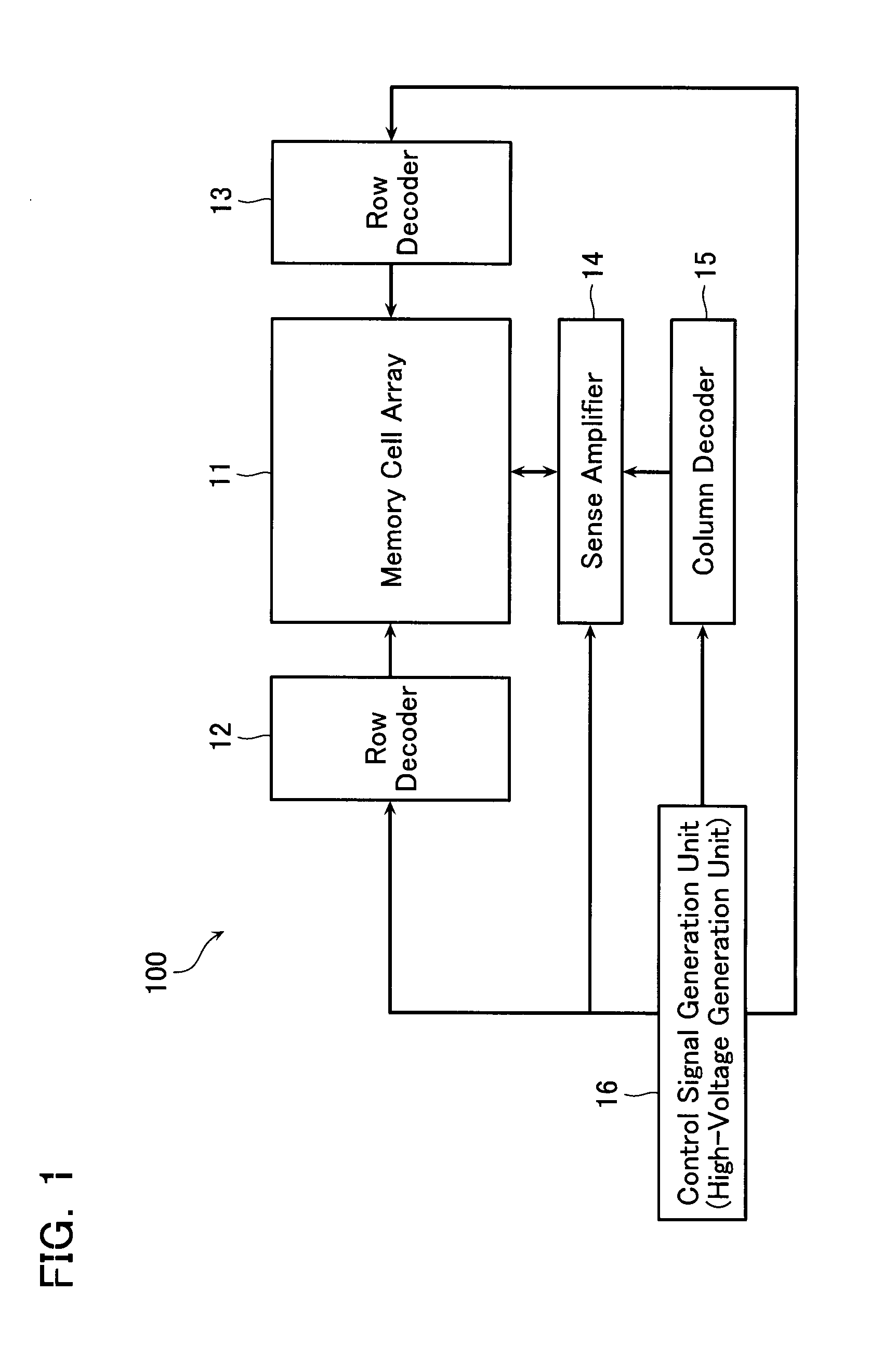
[0038]Referring first to FIG. 1, a configuration of a non-volatile semiconductor storage device 100 according to a first embodiment will be described below. FIG. 1 is a block diagram of the non-volatile semiconductor storage device 100 according to the first embodiment of the present invention.
[0039]As illustrated in FIG. 1, the non-volatile semiconductor storage device 100 of the first embodiment comprises: a memory cell array 11; row decoders 12 and 13; a sense amplifier 14; a column decoder 15; and a control signal generation unit (high-voltage generation unit) 16.
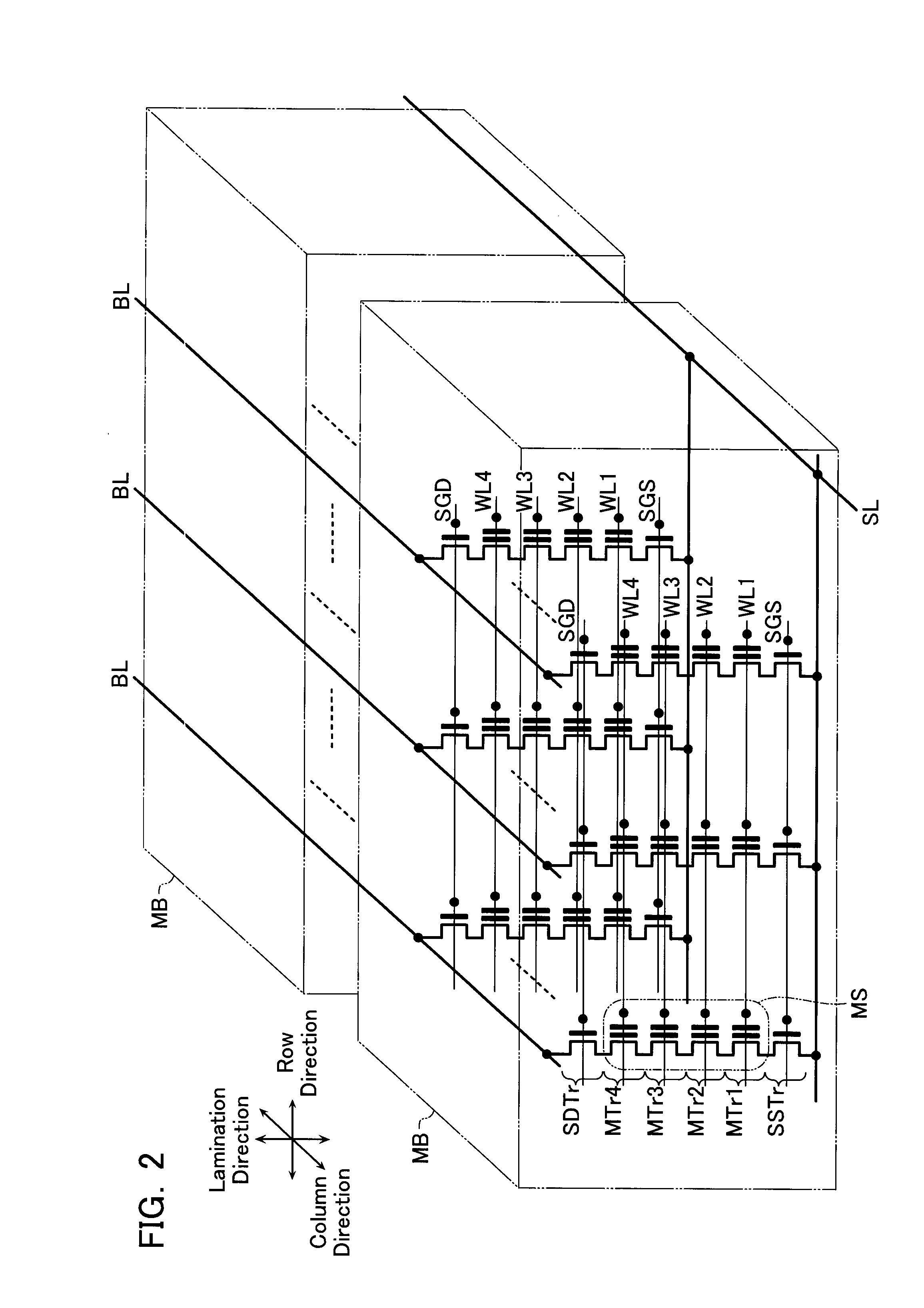
[0040]The memory cell array 11 has memory transistors MTr for electrically storing data. The row decoders 12 and 13 decode captured block address signals and row address signals to control the memory cell array 11. The sense amplifier 14 reads data from the memory cell array 11. The column decoder 15 decodes column address signals to contr...
second embodiment
Configuration of Non-Volatile Semiconductor Storage Device in Second Embodiment
[0096]Referring now to FIG. 14, a configuration of a non-volatile semiconductor storage device according to a second embodiment will be described below. FIG. 14 is a cross-sectional view of the non-volatile semiconductor storage device according to the second embodiment. Note that the same reference numerals represent the same components as the first embodiment and description thereof will be omitted in the second embodiment.
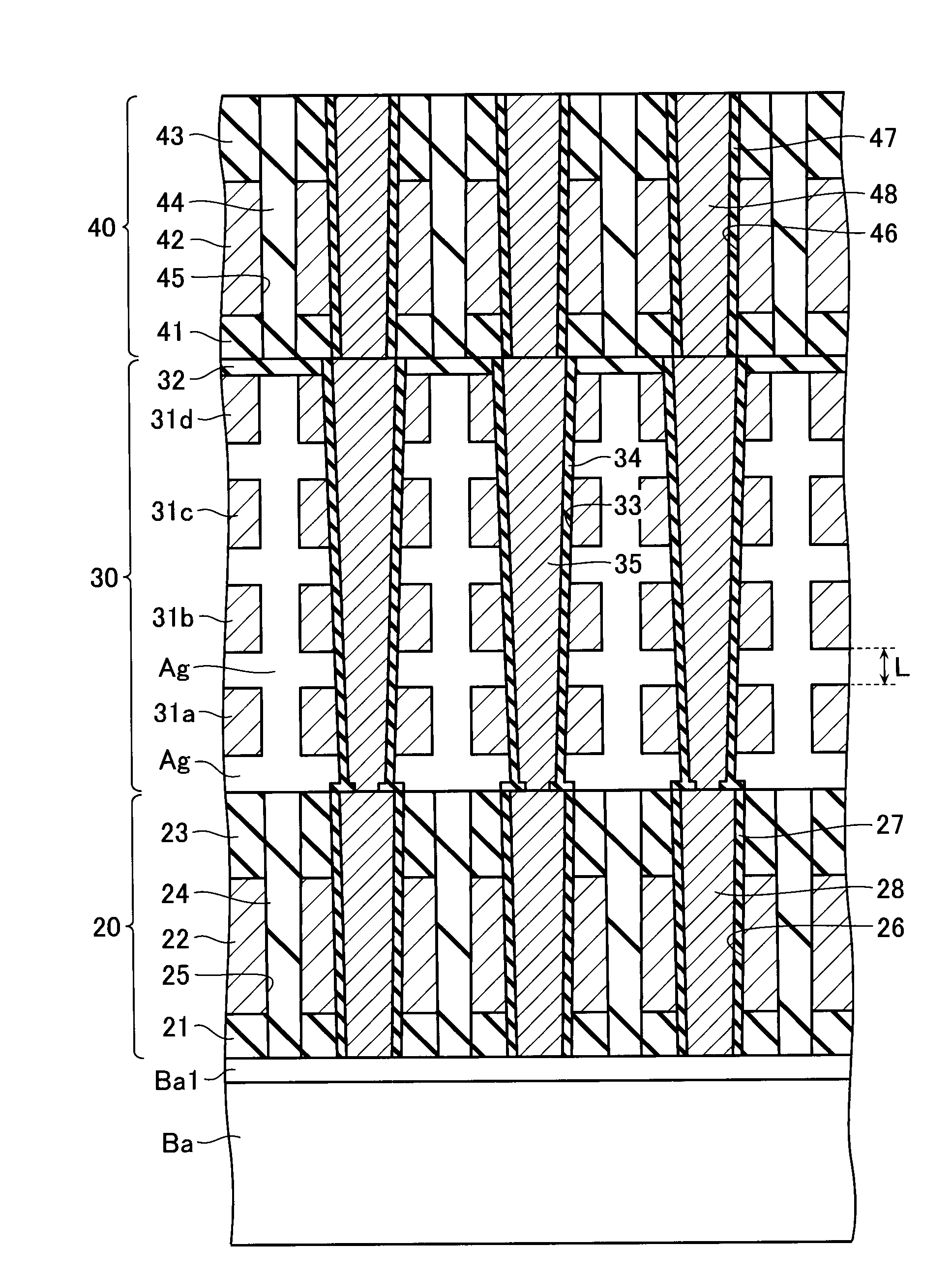
[0097]As illustrated in FIG. 14, the non-volatile semiconductor storage device of the second embodiment comprises a memory transistor layer 30A different from the first embodiment.
[0098]In addition to the configuration of the first embodiment, the memory transistor layer 30A further comprises interlayer insulation layers 36. The interlayer insulation layers 36 are formed to fill up the gaps between the word-line conductive layers 31a to 31d. Each interlayer insulation layer 36 has a c...
PUM
 Abstract
Description
Claims
Application Information