Oled devices

a light-emitting device and blue-oled technology, applied in the direction of organic semiconductor devices, solid-state devices, thermoelectric devices, etc., can solve the problems of adversely affecting charge transport properties, high voltage, and difficult development of efficient blue-oleds based on this technology, so as to improve the balance of electrons and holes, improve the efficiency of oleds, and prevent the conjugation of electrons

Inactive Publication Date: 2010-08-26
BATTELLE MEMORIAL INST
View PDF10 Cites 19 Cited by
  • Summary
  • Abstract
  • Description
  • Claims
  • Application Information

AI Technical Summary

Benefits of technology

[0013]The object of this invention is to improve the efficiency of OLEDs by using a system of materials which includes a novel class of organic phosphoryl compounds which transport both electrons and holes (known as “ambipolar compounds”) to improve the balance of electrons and holes in the recombination region. The system of hole transporting, electron transporting and ambipolar host materials is designed such that there are no large barriers to injection of electrons and holes into the host layer from the electron transporting and hole transporting layers, respectively. To accomplish this, the energy of the LUMO and HOMO in the ambipolar, phosphoryl-containing, host layer is tuned to be close to those of the hole transporting and electron transporting layers, which comprise molecules containing hole transporting groups (HTG) and electron transporting groups (ETG), respectively. The ambipolar host material is created by substituting phosphoryl groups onto the HTG and/or ETG, creating a larger molecule with a HOMO and LUMO very close in energy to that of the unsubstituted molecule. This works because the phos...

Problems solved by technology

Development of efficient blue OLEDs based on this technology, however, has been particularly challenging because the host material must exhibit triplet level emission at ≦470 nm to achieve efficient energy transfer and, furthermore, this high triplet exciton energy must be achieved without sacrificing the good charge transporting properties of the host layer.
Current host materials do not meet these requirements, because there is a tradeoff between increasing the bandgap of the material to increase emission energies and decreasing the π-aromatic system, which may adversely affect charge transport properties.
This leads to a high voltage, particularly at the high current densities required for bright lighting applications, and therefore less efficient devices.
Unfort...

Method used


Image

  • Oled devices
  • Oled devices
  • Oled devices

Examples


Embodiment Construction

[0024]For the purposes of promoting an understanding of the principles of the invention, reference will now be made to the embodiments illustrated in the drawings and specific language will be used to describe the same. It will nevertheless be understood that no limitations of the inventive scope are thereby intended, as the scope of this invention should be evaluated with reference to the claims appended hereto. Alterations and further modifications in the illustrated devices, and such further applications of the principles of the invention as illustrated herein are contemplated as would normally occur to one skilled in the art to which the invention relates.

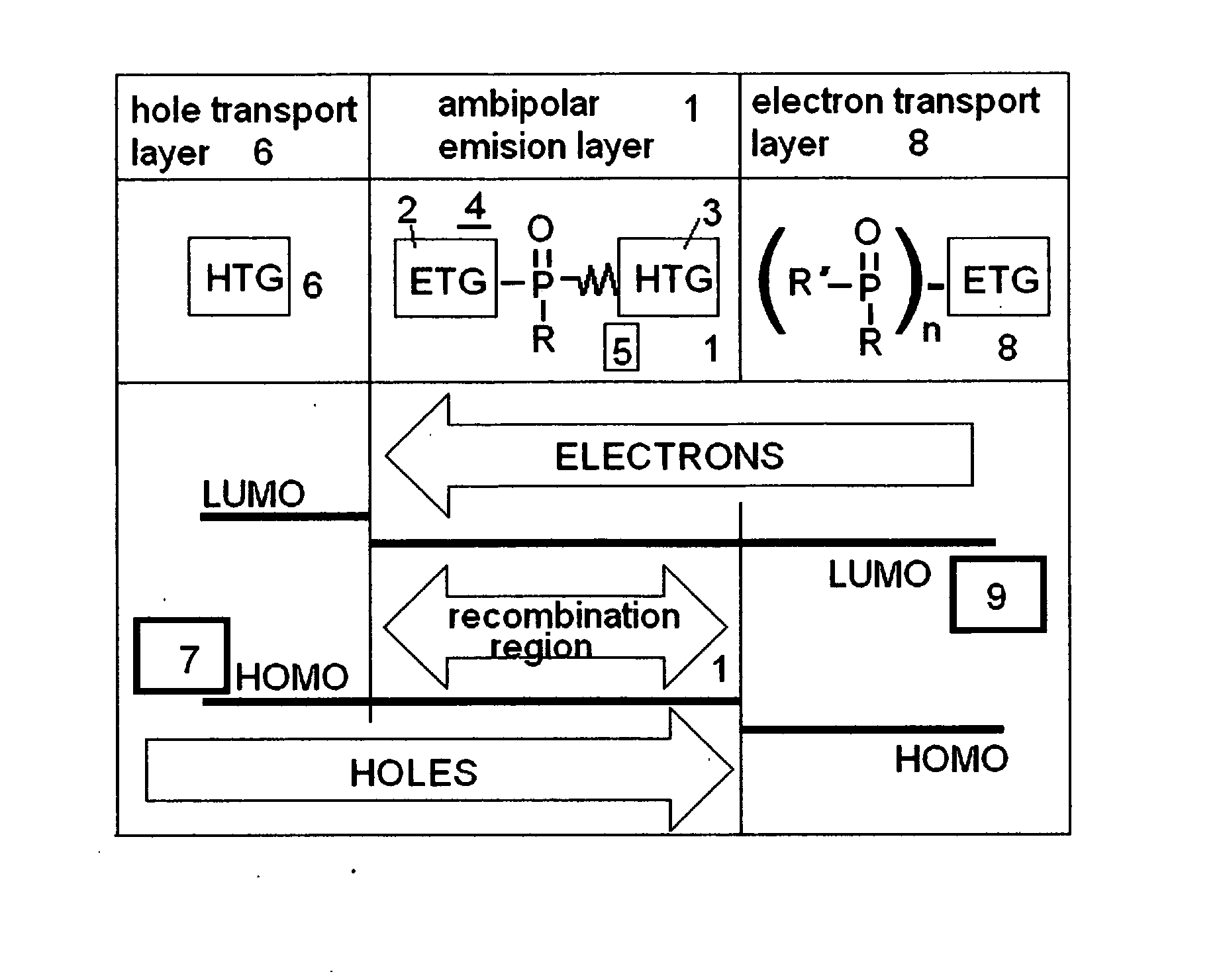
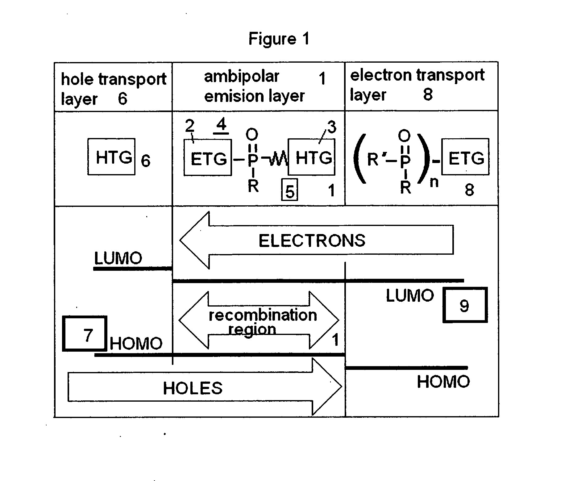
[0025]The concept of a system of layers pertaining to the invention in a three layer device is shown in FIG. 1 which shows molecular designs as schematic block figures in the first row and the resulting alignment of the lowest occupied and highest unoccupied molecular orbitals (LUMO and HOMO, respectively).

[0026]As shown in the...


PUM


Abstract

An OLED device having an emission layer formed of an ambipolar phosphine oxide host material and a dopant, a hole transport layer in electrical communication with an anode, an electron transport layer in communication with a cathode, wherein the HOMO energy of the hole transport layer is substantially the same as the HOMO energy of the ambipolar host in the emission layer, and the LUMO energy of the electron transport layer is substantially the same as the LUMO energy of the ambipolar host in the emission layer.

Description

[0001]The invention was made with Government support under Contract DE-AC0676RLO 1830, awarded by the U.S. Department of Energy. The Government has certain rights in the invention.[0002]Cross Reference to related applications (if any). (Related applications may be listed on an application data sheet, either instead of or together with being listed in the specification.)TECHNICAL FIELD[0003]This invention relates to organic light emitting devices (OLEDs). More specifically, this invention relates to improved OLEDs that are more efficient at converting electrical energy into light than prior art devices.BACKGROUND OF THE INVENTION[0004]Organic light-emitting devices (OLEDs) are electroluminescent devices which contain one or more organic compounds arranged as thin films between two electrodes, one of which is substantially transparent. They are typically deposited in rows and columns onto a flat carrier by evaporation in a vacuum, casting from a solvent or a variety of “printing” proc...

Claims


Application Information

Patent Timeline
IPC IPC(8): H01L51/54
CPCH01L51/0059H01L51/0072H01L2251/552H01L51/5016H01L51/5048H01L51/0074H10K85/631H10K85/6576H10K85/6572H10K50/11H10K2101/10H10K50/14H10K2101/30
Inventor SAPOCHAK, LINDA SUSANBURROWS, PAUL EDWARDBIMALCHANDRA, ASANGA
Owner BATTELLE MEMORIAL INST
Why Eureka
Try Eureka