
Probe for current test, probe assembly and production method thereof

Active Publication Date: 2010-08-26
NIHON MICRONICS
View PDF4 Cites 4 Cited by
  • Summary
  • Abstract
  • Description
  • Claims
  • Application Information

AI Technical Summary

Benefits of technology

[0013]Also, since an adequate amount of solder can be supplied, it does not happen that an excess portion scatters around as heretofore, and it is possible to save the scattered excess portion which would have been discarded heretofore. It is also possible to prevent such environmental pollution as before caused by scattering the excess solder, which dispenses with a particular washing process of machines or instruments to handle the probes and simplifies a production process.
[0014]Further, a portion of the solder melted, for example, by heating can be surely passed around behind the other side face of the probe body through the guide portion. Thus, since the amounts of the melted solder can be approximately uniform by the melted solder flow through the guide portion on both sides of the connection portion, a proper amount of solder can be supplied to the probe connection portion so as to make the amounts of solder approximately uniform on both its sides without causing excess or shortage in supply of the solder. As a result, solder contamination of a probe handling device and probe short circuit due to excessive supply can be prevented, and strength poverty due to shortage in solder can be surely prevented. Also, if the area of the solder layer is selected properly, substantially uniform and proper fillets can be formed on both side faces of the connection portion of the probe body by hardening of the melted solder.
[0015]A solder layer can be provided on each side face of the connection portion of the probe body. In such a case, the thickness of the solder layer or its area can be reduced substantially to half as much as when a solder layer is provided on one side face. For equalization of the solder, it is desirable to provide the solder layers on both side faces of the connection portion. For simplification of the production process of the probes, however, it is desirable to provide the solder layer on one side face of the probe body.
[0016]The solder layer can be formed by a conductive adhesive layer made of a meltable metal material such as simple tin or a tin alloy containing any one or more of gold, silver, cupper and bismuth.
[0017]Also, for the solder layer can be used a plated layer formed by a plating method, for example, by electroforming. Since the thickness of the plating layer can be accurately controlled, the amount of solder to be supplied can be more accurately controlled by forming the solder layer from a plating layer. Thus, since this plating layer can prevent more surely the solder from sticking out, it is particularly effective for the probes arranged at narrow pitches.
[0018]The guide portion can be formed by a concave groove opening in the end face of the connection portion.

Problems solved by technology

It is, however, very difficult to apply a proper amount of cream solder to the connecting end portion of each probe by spraying.
On the other hand, as shown in FIG. 4(c), excessive solder 3 sticking out largely from the wiring land portion 2 causes a short-circuit between the adjacent probes, and the excessive solder scattering around causes a contamination problem to probe handling instruments.
Thus, the supply of the excessive solder brings about various inconveniences.
However, since the tin to be formed on the probe connecting end face is formed by plating, the thickness of the layer is under severe restrictions.
Furthermore, since the area of the connecting end face is small, the connecting end face cannot be enlarged without large-sizing the probe.
Therefore, since it is not possible, by the technique described in the Patent Document 1, to hold a proper amount of solder enough to pass around behind both its side portions of the end face of the probe connection portion, an amount of solder sufficient to obtain a desired connecting strength cannot be supplied to the connection portion of the probe between the probe and the probe board.

Method used


Image

  • Probe for current test, probe assembly and production method thereof
  • Probe for current test, probe assembly and production method thereof
  • Probe for current test, probe assembly and production method thereof

Examples


Embodiment Construction

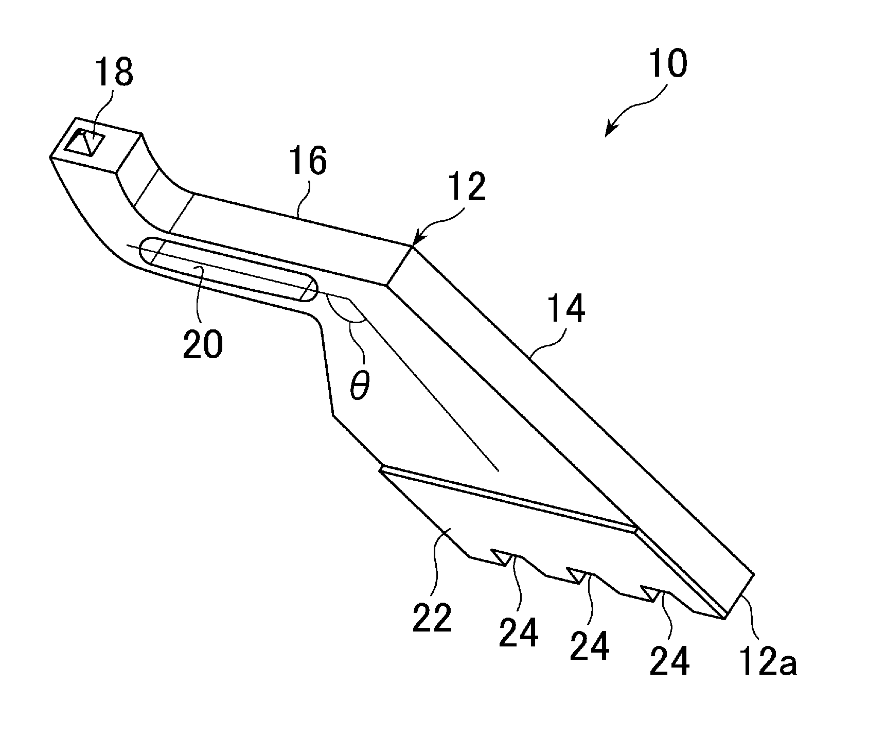
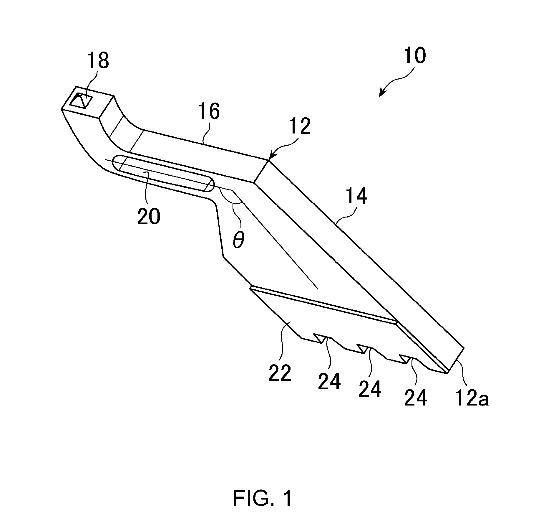
[0037]The probe 10 according to the present invention is, as shown in FIG. 1, provided with a generally plate-like probe body 12. The probe body 12 has: a flat rectangular end face 12a which is used as a connection face to a wiring path described later; a plate-like connection portion 14 rising angularly from the end face; and an arm portion 16 extending at an obtuse angle θ in a direction approximately parallel to the longitudinal direction of the end face 12a from the front end of the connection portion 14 on a plane including the connection plane to a wiring path to be described later. The front end portion of the arm portion 16 rises in a direction to be away from the end face 12a of the connection portion 14, and a tip 18 is formed at the front end face.

[0038]The probe body 12 except the tip 18 is made of a highly tough metal material such as, for example, nickel, its alloy or phosphor bronze. In the illustration, in order to enhance the flexibility of the arm portion 16, a lon...


PUM


Abstract

A probe for current test comprising: a probe body having a plate-like connection portion whose end face becomes a connection face to a probe board; a solder layer formed on at least one side face of said connection portion; and a guide portion formed on the connection portion, penetrating the connection portion in its thickness direction from the one side face with the solder layer formed to the other side face, and when the solder layer is melted, capable of guiding a portion thereof to the other side face.

Description

TECHNICAL FIELD[0001]The present invention relates to a probe, a probe assembly suitable for a current test of semiconductor devices such as semiconductor integrated circuits and a method for producing them.BACKGROUND[0002]Semiconductor devices such as multiple semiconductor integrated circuits formed on each chip region of a semiconductor wafer undergo a current test to determine whether or not each of them is produced according to its specification. In this type of current test is used a probe assembly generally called probe card. When the plural probes (contacts) provided on a probe board of this probe assembly are pressed against their corresponding electrodes of a device under test, the device under test is connected to a tester through the probe assembly.[0003]In this probe assembly, the probe is connected to each attaching land portion provided at a wiring circuit of the probe board.[0004]In a conventional production of a probe assembly, lead-free cream solder containing mult...

Claims


Application Information

Patent Timeline
IPC IPC(8): G01R31/02G03F7/20
CPCG01R1/06733G01R1/06727G01R3/00G01R1/06761G01R1/073
Inventor SOUMA, AKIRAURUSHIYAMA, YOSHIKAZUTAZAWA, MASAHISASATO, TOMOYAHIRAKAWA, HIDEKIHAYASHIZAKI, TAKAYUKI
Owner NIHON MICRONICS
Learn More