Semiconductor device manufacturing method

a semiconductor device and manufacturing method technology, applied in the direction of coatings, chemical vapor deposition coatings, electric discharge tubes, etc., can solve the problems of deteriorating the quality of the semiconductor device, increasing the effect of plasma damage accompanied by accumulation of charges, and mos transistors with plasma damage, so as to reduce the effect of plasma damage on the semiconductor elemen

Active Publication Date: 2010-08-26
TOKYO ELECTRON LTD +1
View PDF3 Cites 6 Cited by
  • Summary
  • Abstract
  • Description
  • Claims
  • Application Information

AI Technical Summary

Benefits of technology

[0010]To solve the above and/or other problems, the present invention provides a semiconductor device manufacturin

Problems solved by technology

Here, when the plasma process is performed on a silicon substrate (wafer) by using each of the plasma, electric charges are accumulated in a gate oxide film (gate insulation film) or adjacent layer included in a MOS transistor, and thus the MOS transistor has plasma damage, such as a charge-up.
When the MOS transistor has plasma damage, threshold value voltage (Vth) shift deviation or reduced current driving capability is occurred, thereby deteriorating the quality of the semiconductor device.
However, as a smaller gate area of a transistor and a thinner film are required according to the development of a technology for minutely processing an LSI c

Method used


Image

  • Semiconductor device manufacturing method
  • Semiconductor device manufacturing method
  • Semiconductor device manufacturing method

Examples


Embodiment Construction

[0038]Hereinafter, the present invention will be described in detail by explaining exemplary embodiments of the invention with reference to the attached drawings.

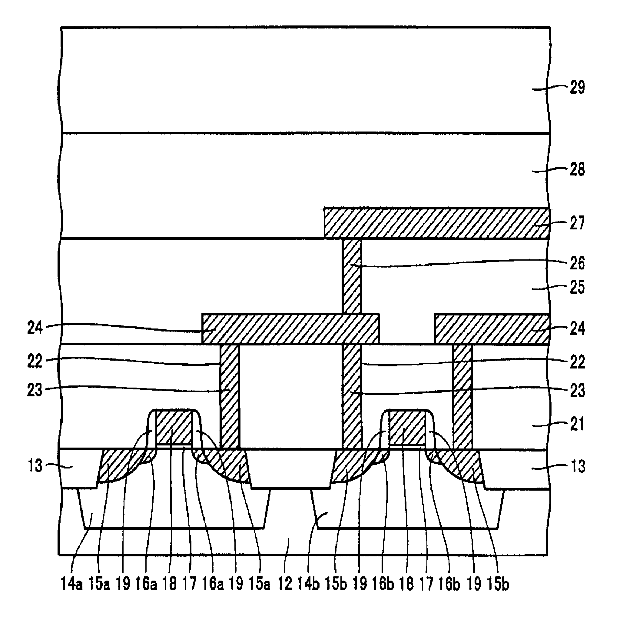
[0039]FIG. 1 is a cross-sectional view of a part of a semiconductor device manufactured according to a semiconductor device manufacturing method, according to an embodiment of the present invention.

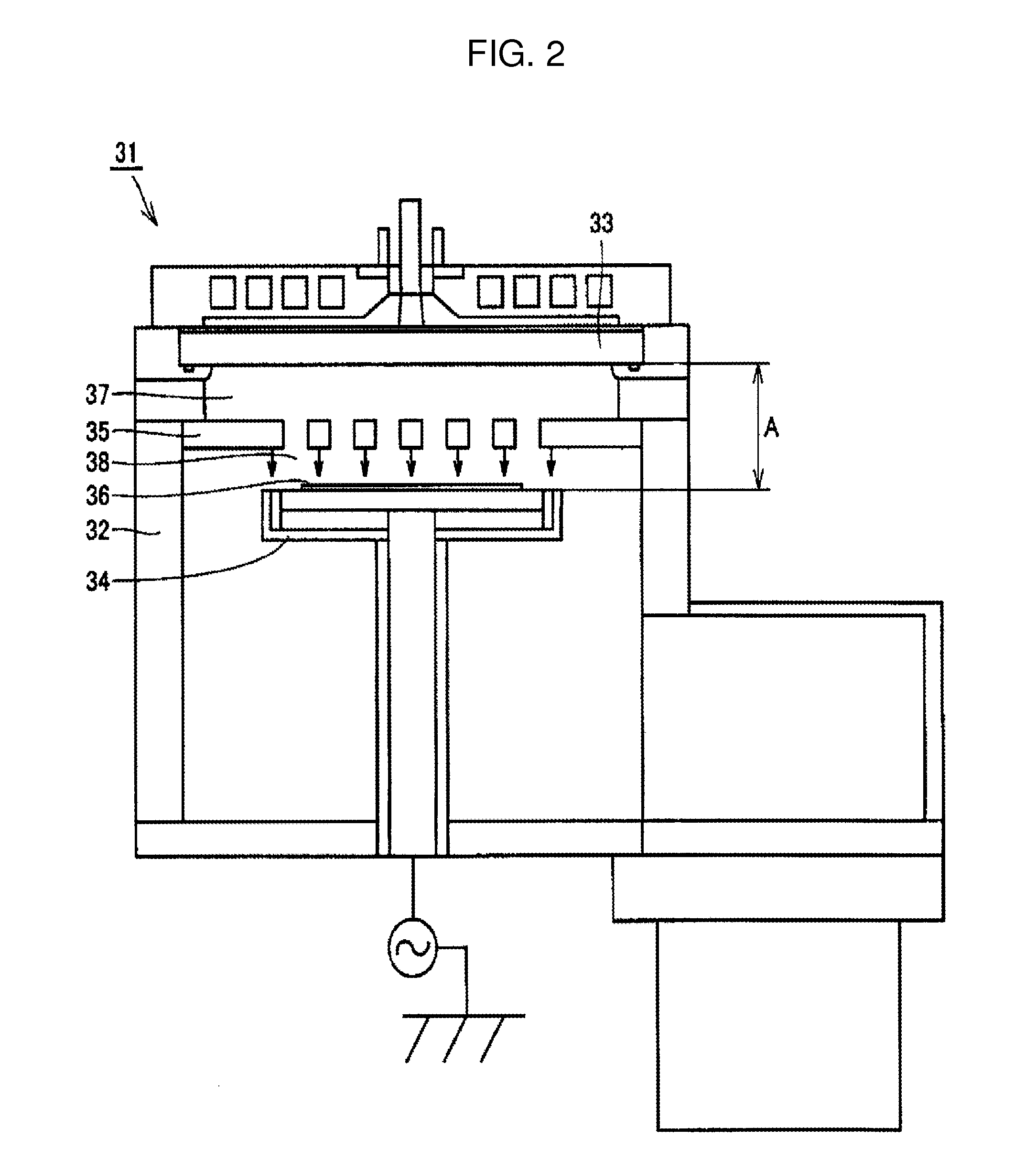
[0040]According to an embodiment of the present invention, a metal oxide semiconductor transistor (MOS) is described as a semiconductor device and a microwave plasma processing apparatus is explained as a plasma processing apparatus. Also in FIG. 1, conductive layers are shown in hatching.

[0041]Referring to FIG. 1, a device isolating region 13, a p-type well 14a, an n-type well 14b, a highly-concentrated n-type impurity diffusion region 15a, a highly-concentrated p-type impurity diffusion region 15b, an n-type impurity diffusion region 16a, and a p-type impurity diffusion region 16b are formed on a silicon substrate 12. Since a m...


PUM

PropertyMeasurementUnit
Energyaaaaaaaaaa
Carrier concentrationaaaaaaaaaa
Electron concentrationaaaaaaaaaa

Abstract

A semiconductor device manufacturing method, the method including: forming a semiconductor element on a semiconductor substrate; and by using microwaves as a plasma source, forming an insulation film on the semiconductor element by performing a CVD process using microwave plasma having an electron temperature of plasma lower than 1.5 eV and an electron density of plasma higher than 1×1011 cm−3 near a surface of the semiconductor substrate.

Description

TECHNICAL FIELD[0001]The present invention relates to a semiconductor device manufacturing method, and more particularly, to a semiconductor device manufacturing method, the method including forming a semiconductor element on a semiconductor substrate, and then forming an insulation layer and a conductive layer on the semiconductor element by using plasma.BACKGROUND ART[0002]Semiconductor devices, such as large scale integrated circuits(LSI), are manufactured via a plurality of processes, such as etching, chemical vapor deposition (CVD), and sputtering, performed with respect to a silicon substrate. These processes, such as etching, CVD, and sputtering, may use plasma as an energy supply source, that is, may be plasma etching, plasma CVD, and plasma sputtering.[0003]When manufacturing a semiconductor device, plasma processes described above are effectively used along with recent miniaturization or multilayered-wiring of LSI. For example, when performing a plasma process for manufact...

Claims


Application Information

Patent Timeline
IPC IPC(8): H01L21/28
CPCC23C16/511H01J37/32192H01L21/31116H01L21/02274H01L21/31055H01L21/02164H01L21/205H01L21/3205
Inventor UEDA, HIROKAZUNOZAWA, TOSHIHISAMATSUOKA, TAKAAKITERAMOTO, AKINOBUOHMI, TADAHIRO
Owner TOKYO ELECTRON LTD
Why Eureka
Try Eureka