Scanning probe microscope and method of observing sample using the same

a probe microscope and probe technology, applied in the field of scanning probe microscopes, can solve the problems of limited apertures to several tens of nm, and achieve the effects of reducing the reproducibility of measured images, difficult stably forming apertures, and extremely low measurement repeatability

Active Publication Date: 2010-08-26
HITACHI LTD
View PDF4 Cites 28 Cited by
  • Summary
  • Abstract
  • Description
  • Claims
  • Application Information

AI Technical Summary

Benefits of technology

[0010]However, measurement resolution of the above-described scanning near-field optical microscope is the order of several tens of nm, and the resolution is lower, by an order of magnitude or more, than those of an atomic force microscope and electron microscope having a resolution on the order of nm. Also, the scanning near-field optical microscope has a problem of extremely-low measurement repeatability which is critical

Problems solved by technology

Also, the scanning near-field optical microscope has a problem of extremely-low measurement repeatability which is critical for industrial application.
That is, in the method using an aperture probe among the methods described above, it is extremely difficult to stably form the aperture, and the aperture is practically limited to several tens of nm.
Further, the tip portion is damaged or worn by hitting of the probe to the sample when scanning over the sample to widen the aperture, and therefore, reproducibility of the measured image is decreased.
On the other hand, while the scattering probe using a metal probe has a higher resolution than that of the aperture probe, the scattering probe has problems that external lighting is scattered on a base of the probe or the surface of the sample to become background noise, or that the tip portion is damaged or worn by hitting of the probe to the sample when scanning over th

Method used


Image

  • Scanning probe microscope and method of observing sample using the same
  • Scanning probe microscope and method of observing sample using the same
  • Scanning probe microscope and method of observing sample using the same

Examples


first embodiment

[0058]A first embodiment of the present invention is described with reference to FIGS. 1 to 20.

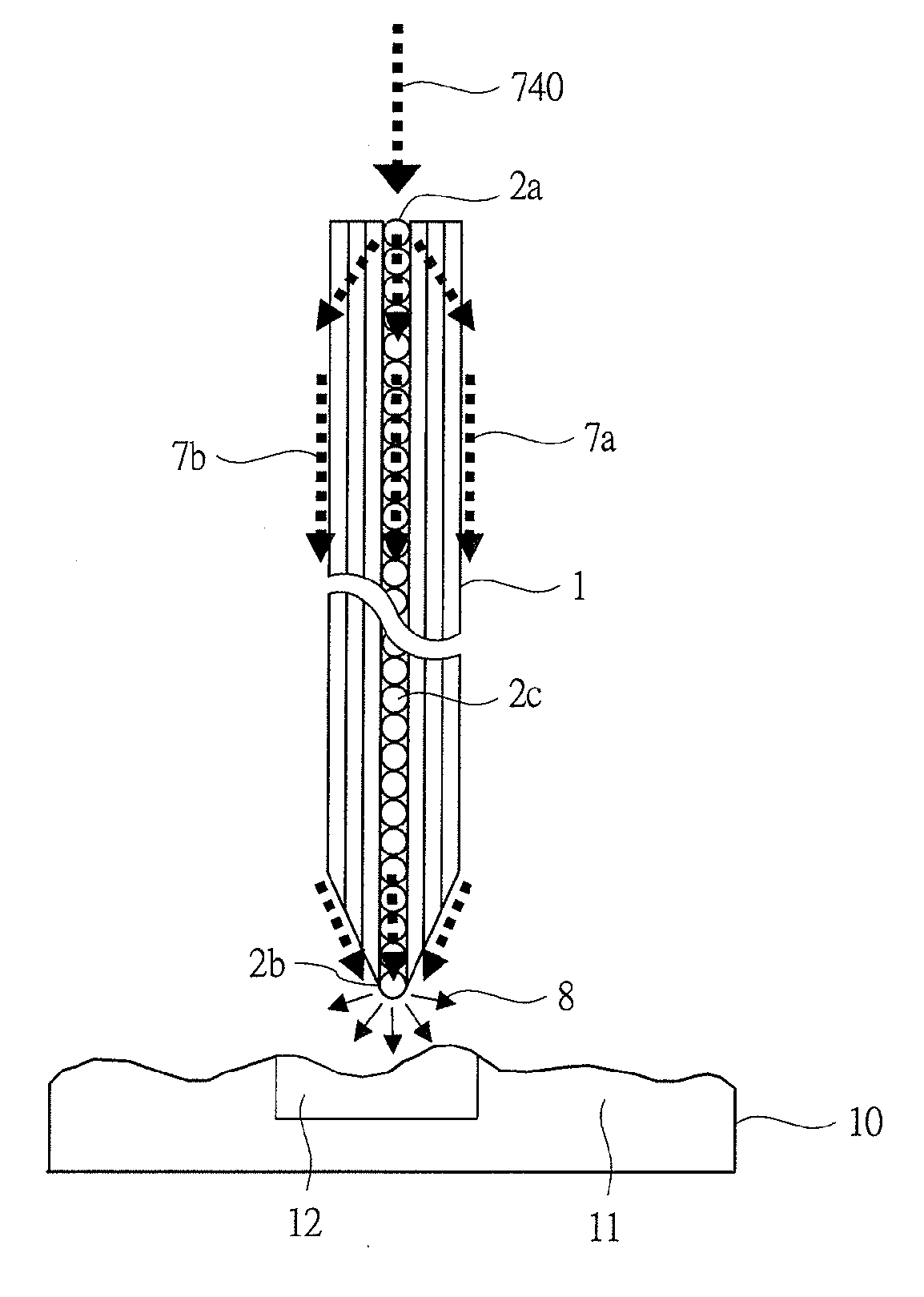
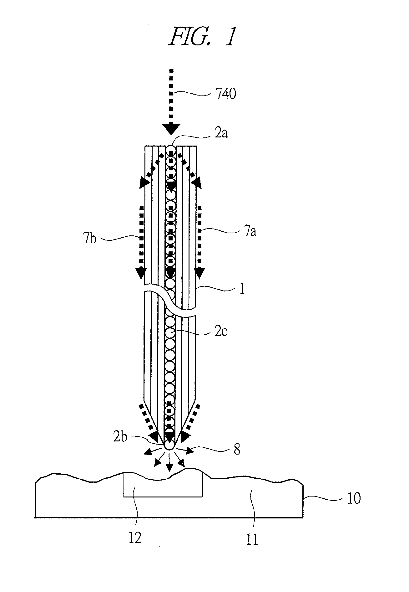
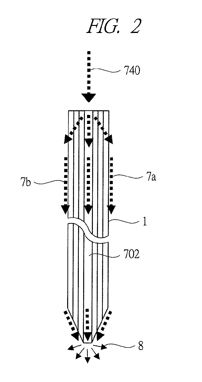
[0059]First, a configuration of a plasmon-enhanced near-field probe according to the present embodiment is described with reference to FIGS. 1 to 3. In the present embodiment, as illustrated in FIG. 1, the plasmon-enhanced near-field probe is formed by sharpening a bottom end portion in a nanotube 1 as a circular cone shape, the nanotube 1 such as a multilayered carbon nanotube (CNT), a metal nanotube, or a boron nitride (BN) nanotube having properties as an insulator, and by filling spherical gold nano-particles 2 (2a, 2c, and 2b) made of gold (Au) in a top end portion, an inside, and a bottom end portion of a hollow portion inside the nanotube 1.

[0060]For example, a voltage is applied to both ends of the nanotube, 1 such as a carbon nanotube, and a current is saturated in time as increasing the applied voltage. As further increasing the applied voltage, the current is decreased step by s...

second embodiment

[0130]A second embodiment according to the present invention is described with reference FIG. 21. FIG. 21 illustrates, in the plasmon exciting unit 200 according to the present embodiment, a method of fixing the nanotube 1 to the chip 730 and a principle of guiding the excited TM mode plasmon 740 toward the nanotube 1. In the plasmon exciting unit according to the first embodiment described above, three gold dots 750a are formed by the irradiation of electron beams, and these gold dots are used as a binder to be melted to adhere the nanotube 1 on the tip of the chip 730. Also, in consideration of ensuring sufficient strength for the fixing and achieving the coupling efficiency of the plasmon to the nanotube having a diameter of 20 nm, it is set in the first embodiment described above such that D=40 nm, H=40 nm, and the distance P=250 nm.

[0131]In the present embodiment, for the gold dot 750a at the incident end portion in the nanotube 1, it is set such that D=40 nm and H=40 nm in con...

third embodiment

[0135]A third embodiment according to the present invention is described with reference FIG. 22. FIG. 22 illustrates, in the plasmon exciting unit 200 according to the present embodiment, a method of fixing the nanotube 1 to the chip 730 and a principle of guiding the excited TM mode plasmon 740 toward the nanotube 1. In the plasmon exciting unit according to the first embodiment described above, three gold dots 750a are formed by the irradiation of electron beams, and these gold dots are used as a binder to be melted to adhere the nanotube 1 on the tip of the chip 730. Also, in consideration of ensuring sufficient strength for the fixing and achieving the coupling efficiency of the plasmon to the nanotube having a diameter of 20 nm, it is set in the first embodiment described above such that D=40 nm, H=40 nm, and the distance P=250 nm.

[0136]In the present embodiment, for the gold dot 750a at the incident end portion in the nanotube 1, it is set such that D0=40 nm and H0=40 nm in co...


PUM


Abstract

In a scanning probe microscope, a nanotube and metal nano-particles are combined together to configure a plasmon-enhanced near-field probe having an optical resolution on the order of nanometers as a measuring probe in which a metal structure is embedded, and this plasmon-enhanced near-field probe is installed in a highly-efficient plasmon exciting unit to repeat approaching to and retracting from each measuring point on a sample with a low contact force, so that optical information and profile information of the surface of the sample are measured with a resolution on the order of nanometers, a high S/N ratio, and high reproducibility without damaging both of the probe and the sample.

Description

CROSS-REFERENCE TO RELATED APPLICATION[0001]The present application claims priority from Japanese Patent Application No. JP 2009-042242 filed on Feb. 25, 2009, the content of which is hereby incorporated by reference into this application.TECHNICAL FIELD OF THE INVENTION[0002]The present invention relates to a scanning probe microscope technique and a technique effectively applied to a method of observing a sample using the scanning probe microscope.BACKGROUND OF THE INVENTION[0003]Scanning probe microscopes (SPMs) have been known as a technique of measuring a fine three-dimensional shape. Among the scanning probe microscopes, anatomic force microscope (AFM) is an observation technique of scanning a surface of a sample while keeping a contact force at a very small value by controlling a probe with a pointed tip, and is widely used as a technique measurable for a fine three-dimensional shape on the order of atom. However, this atomic force microscope cannot measure optical properties...

Claims


Application Information

Patent Timeline
IPC IPC(8): G01Q20/02G01Q60/18
CPCB82Y15/00B82Y20/00G01Q70/12G01Q60/22B82Y35/00
Inventor NAKATA, TOSHIHIKOWATANABE, MASAHIROINOUE, TAKASHIHIDAKA, KISHIOOKAI, MAKOTOHIROOKA, MOTOYUKI
Owner HITACHI LTD
Why Eureka
Try Eureka