Photovoltaic converter device and electronic device

a converter device and photovoltaic technology, applied in semiconductor devices, material nanotechnology, nanotechnology, etc., can solve the problems of extremely difficult and ineffective charge (electrons) retrieval from quantum wells, and achieve the effect of improving the character of the electronic apparatus

Active Publication Date: 2010-09-09
SEIKO EPSON CORP
View PDF5 Cites 22 Cited by
  • Summary
  • Abstract
  • Description
  • Claims
  • Application Information

AI Technical Summary

Benefits of technology

[0016]An electronic apparatus in accordance with another aspect of the invention includes any one of the photovoltaic con...

Problems solved by technology

However, with the structure using silicon as the quantum dots that are examined in detail in the above-mentioned Patent Document 1 and silicon oxide as the dielectric material thin layers, it is feared that charge (electrons) cannot...

Method used


Image

  • Photovoltaic converter device and electronic device
  • Photovoltaic converter device and electronic device
  • Photovoltaic converter device and electronic device

Examples


Embodiment Construction

[0034]Preferred embodiments of the invention are described in detail below with reference to the accompanying drawings. It is noted that components having the same function shall be appended with the same or related reference numbers, and their description shall not be repeated.

[0035]Structure of Photovoltaic Converter Device>

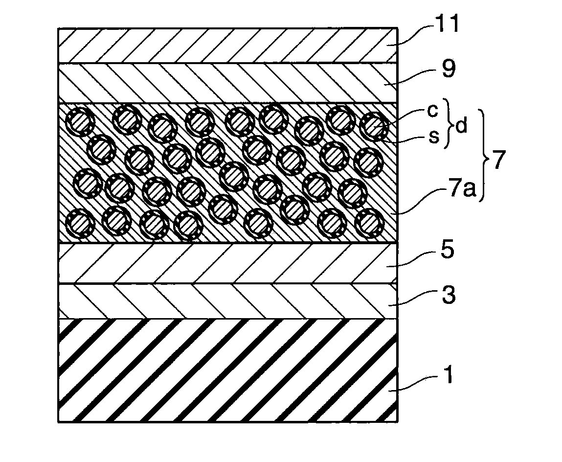
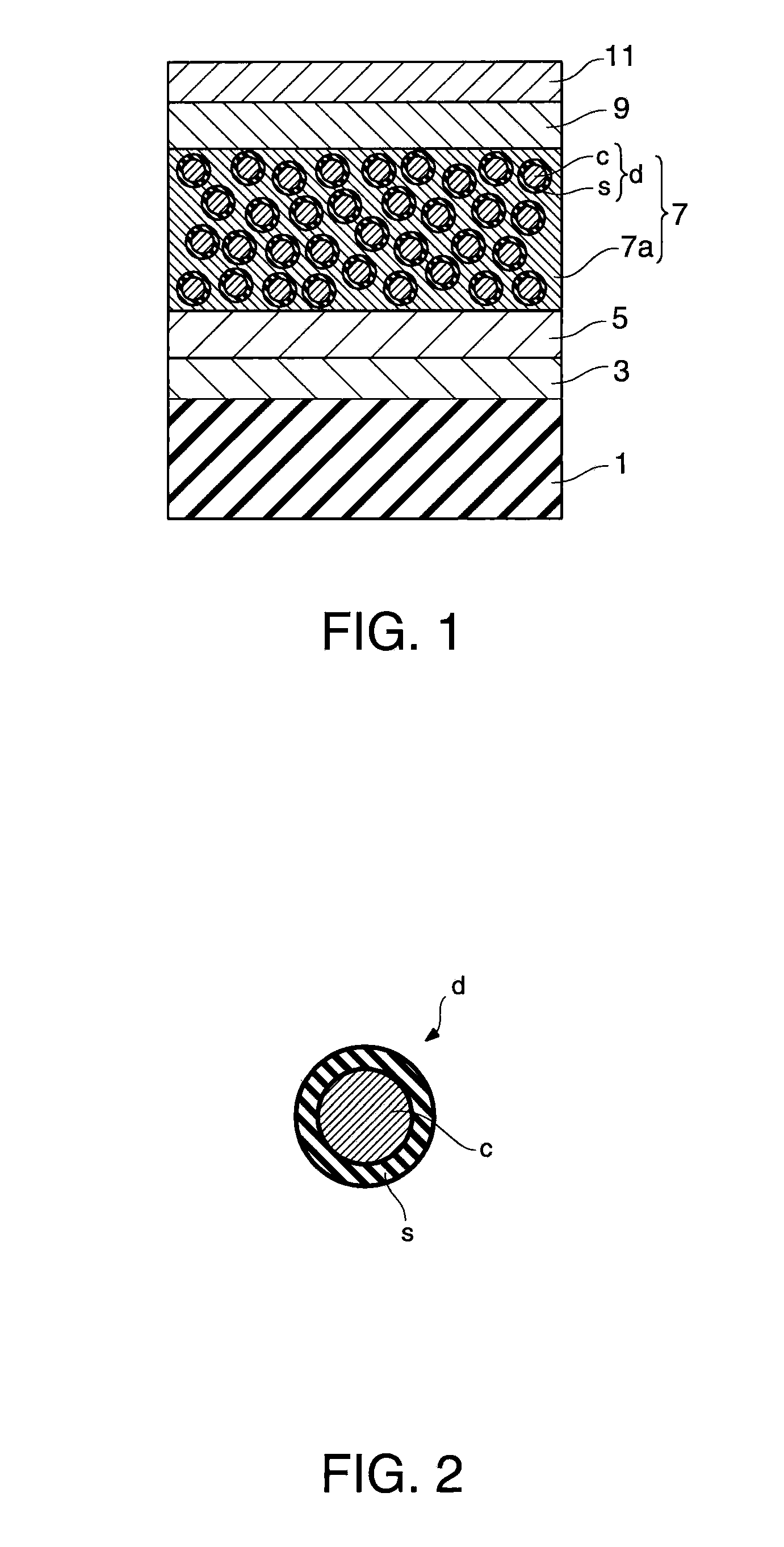
[0036]FIG. 1 is a cross-sectional view showing the structure of a quantum dot type photovoltaic converter device (a photovoltaic converter element, a solar cell) in accordance with an embodiment of the invention. FIG. 2 is a cross-sectional view showing the structure of a quantum dot d shown in FIG. 1.

[0037]The photovoltaic converter device shown in FIG. 1 is a device with a so-called pin structure, and has a structure in which a p-layer, an i-layer and an n-layer are sequentially laminated. More specifically, as shown in the figure, on a substrate 1, a transparent electrode 3, a p-type (first conductivity type) amorphous silicon layer 5, an i-layer 7, an n-typ...


PUM


Abstract

A photovoltaic converter device includes a photovoltaic conversion layer containing a plurality of nanoparticles in a first material in a dispersed state, wherein the nanoparticles include a second material in particles and a third material that coats the second material, the third material having a band gap E3 that is greater than a band gap E1 of the first material, and greater than a band gap E2 of the second material.

Description

[0001]The entire disclosure of Japanese Patent Application No. 2009-050922, filed Mar. 4, 2009 is expressly incorporated by reference herein.BACKGROUND[0002]1. Technical Field[0003]The present invention relates to photovoltaic converter devices and, in particular, to photovoltaic converter devices that use nanoparticles.[0004]2. Related Art[0005]As clean energy sources that contribute to energy conservation and resource saving, solar cells (i.e., photovoltaic converter devices) are being actively developed. Solar cells are electric power devices that use the photo-electromotive force effect to directly convert light energy to electric power. As their structures, various kinds of structures, such as, organic thin film solar cells, dye-sensitized solar cells, solar cells with multi-junction structure, and the like are being investigated. Above all, solar cells that use quantum dots (nanoparticles) are attracting attention as the next-generation solar cells that make it possible in the...

Claims


Application Information

Patent Timeline
IPC IPC(8): H01L31/00
CPCB82Y10/00Y10S977/948H01L21/0245H01L21/02513H01L21/02521H01L21/02532H01L21/02546H01L21/0256H01L21/02568H01L21/02592H01L21/02601H01L31/0352H01L31/035236H01L31/0384H01L31/075Y02E10/548B82Y30/00H01L31/035218Y10S977/774B82Y20/00
Inventor FURUSAWA, MASAHIRO
Owner SEIKO EPSON CORP
Why Eureka
Try Eureka