

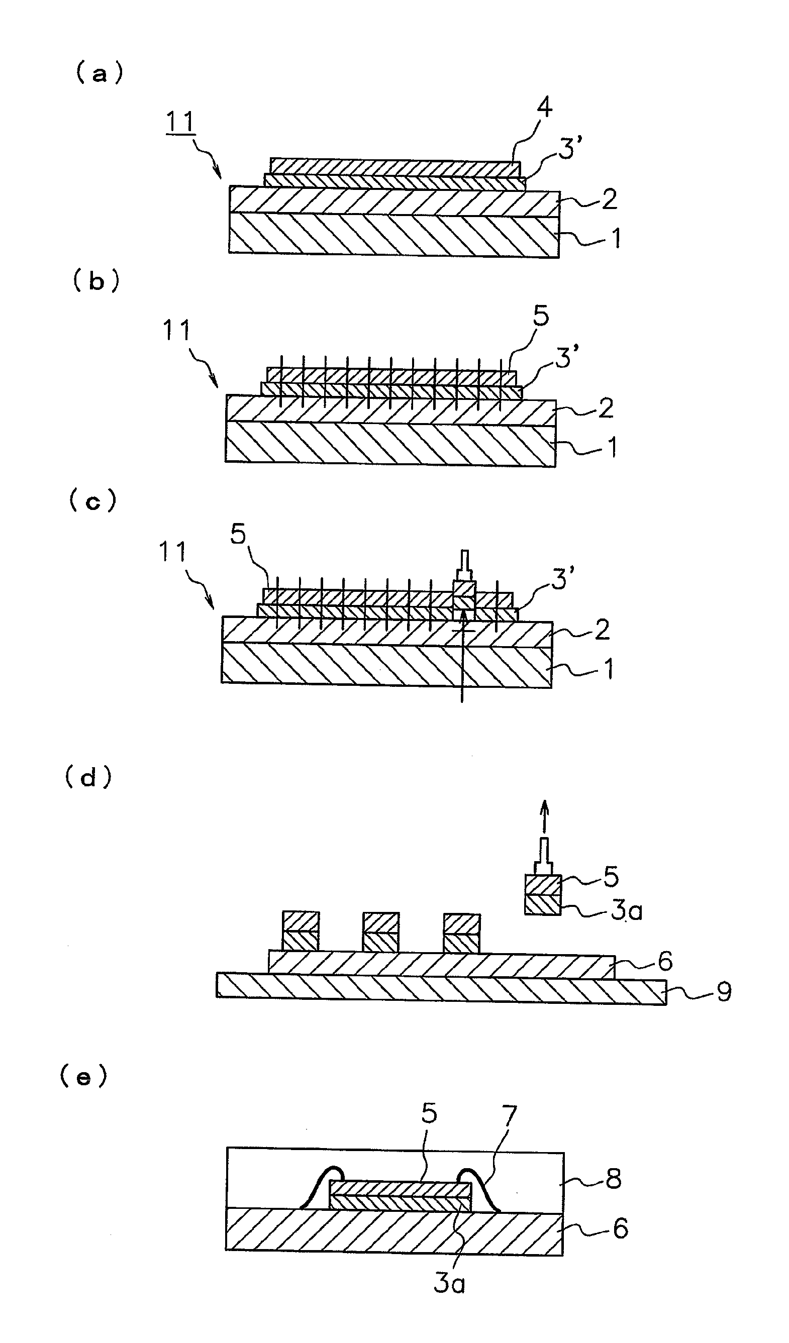
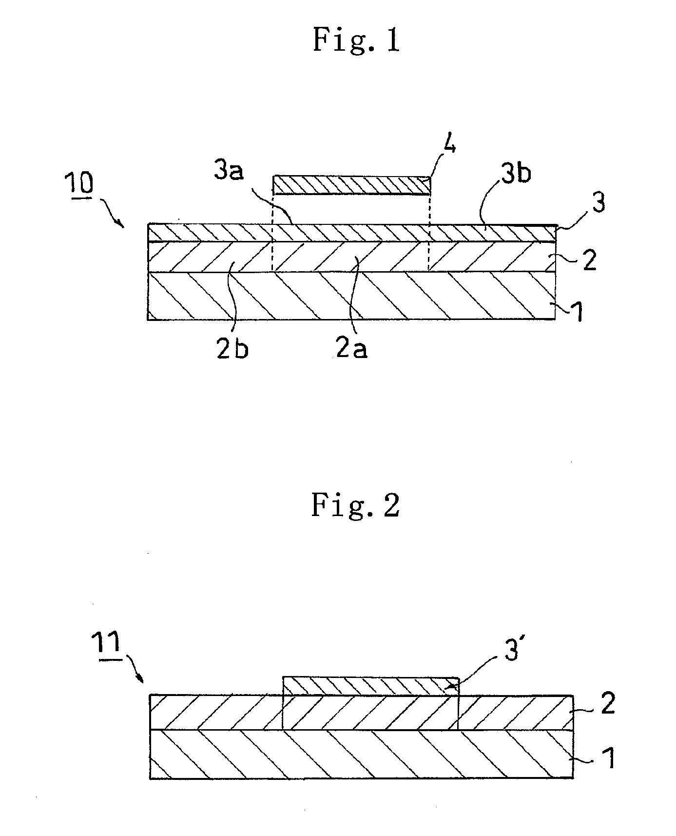
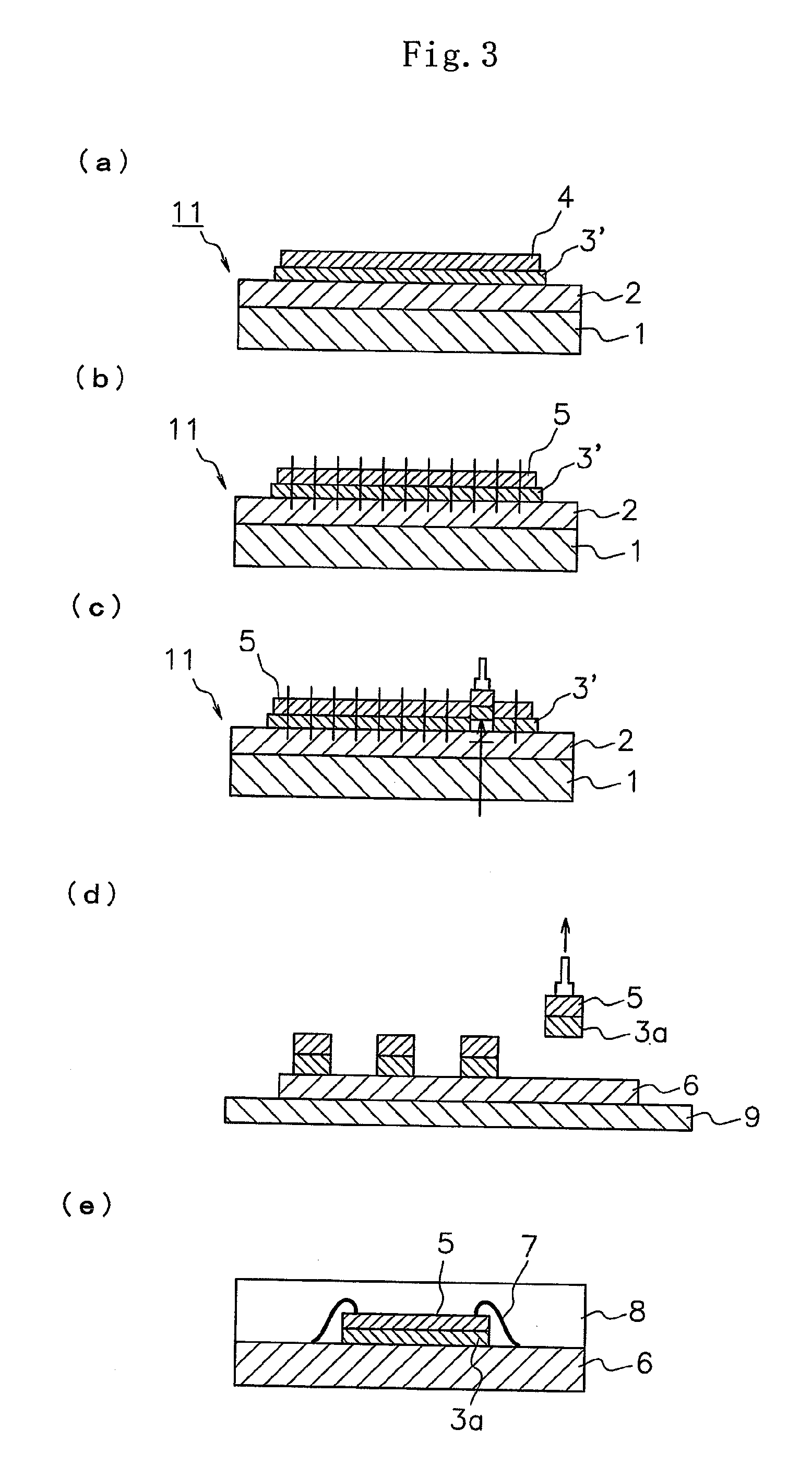
Dicing die-bonding film
a die-bonding film and die-bonding technology, applied in the direction of film/foil adhesives, synthetic resin layered products, transportation and packaging, etc., can solve the problems of difficult uniformity of adhesive layers, long time-consuming and labor-intensive, and special equipment, so as to prevent formation of low molecular weight polymers, prevent peeling from dicing rings, and prevent insufficient crosslinking
- Summary
- Abstract
- Description
- Claims
- Application Information
AI Technical Summary
Benefits of technology
Problems solved by technology
Method used
Image

Examples
example 1
Manufacture of Dicing Film
[0091]An acryl polymer A having a weight average molecular weight of 850,000 was obtained by charging 88.8 parts of 2-ethylhexylacrylate (hereinbelow, refers to as “2EHA”), 11.2 parts of 2-hydroxyethylacrylate (hereinbelow, referred to as “HEA”), 0.2 parts of benzoylperoxide, and 65 parts of toluene into a reactor equipped with a condenser, a nitrogen introducing pipe, a thermometer, and a stirring apparatus, and performing a polymerization process at 61° C. for 6 hours in a nitrogen flow. The weight average molecular weight is as described below. The molar ratio of 2EHA and HEA was made to be 100 mol to 20 mol.
[0092]An acryl polymer A′ was obtained by adding 12 parts of 2-methacryloyloxyethylisocyanate (hereinbelow, referred to as “MOI”) (80 mol % to HEA) to the acryl polymer A and performing an addition reaction process at 50° C. for 48 hours in an air flow.
[0093]Next, a pressure-sensitive adhesive solution was manufactured by adding 8 parts of a polyisoc...
examples 2 to 15
[0108]A dicing die-bonding film was manufactured in each of examples 2 to 15 in the same manner as in the example 1 except that the composition and the content were changed to the values shown in Table 1 below.
TABLE 1Hydroxyl group-containingIsocyanateAcrylic acid estermonomercompoundPhotopolymerization2EHAi-OAi-NABALAAAHEA4HBAMOIAOITolueneC / LT / CinitiatorExample 188.8—————11.2—12—658—5(100)(20)(80)Example 293 —————7 — 7.8—658—5(100)(12)(83)Example 384.1—————15.9—17—658—5(100)(30)(80)Example 4—88.8————11.2—12—658—5(100)(20)(80)Example 5——89.5——10.5— 11.2—658—5(100)(20)(80)Example 661.8——25.8——12.5— 13.3—658—5 (62.5)(37.5)(20)(80)Example 789.5——————10.5 9.1—658—5(100)(15)(80)Example 888.8—————11.2——10.9658—5(100)(20)(80)Example 988.8—————11.2— 10.5—658—5(100)(20)(70)Example 1088.8—————11.2— 13.5—658—5(100)(20)(90)Example 1191.1————0.3 8.6— 10.4—65—0.55(100)(0.8)(15)(90)Example 1288.8—————11.2—12—1008—5(100)(20)(80)Example 1388.8—————11.2—12—408—5(100)(20)(80)Example 1488.8——...
PUM
| Property | Measurement | Unit |
|---|---|---|
| tensile elastic modulus | aaaaa | aaaaa |
| tensile elastic modulus | aaaaa | aaaaa |
| thickness | aaaaa | aaaaa |
Abstract
Description
Claims
Application Information