

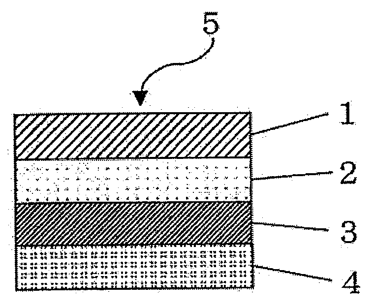
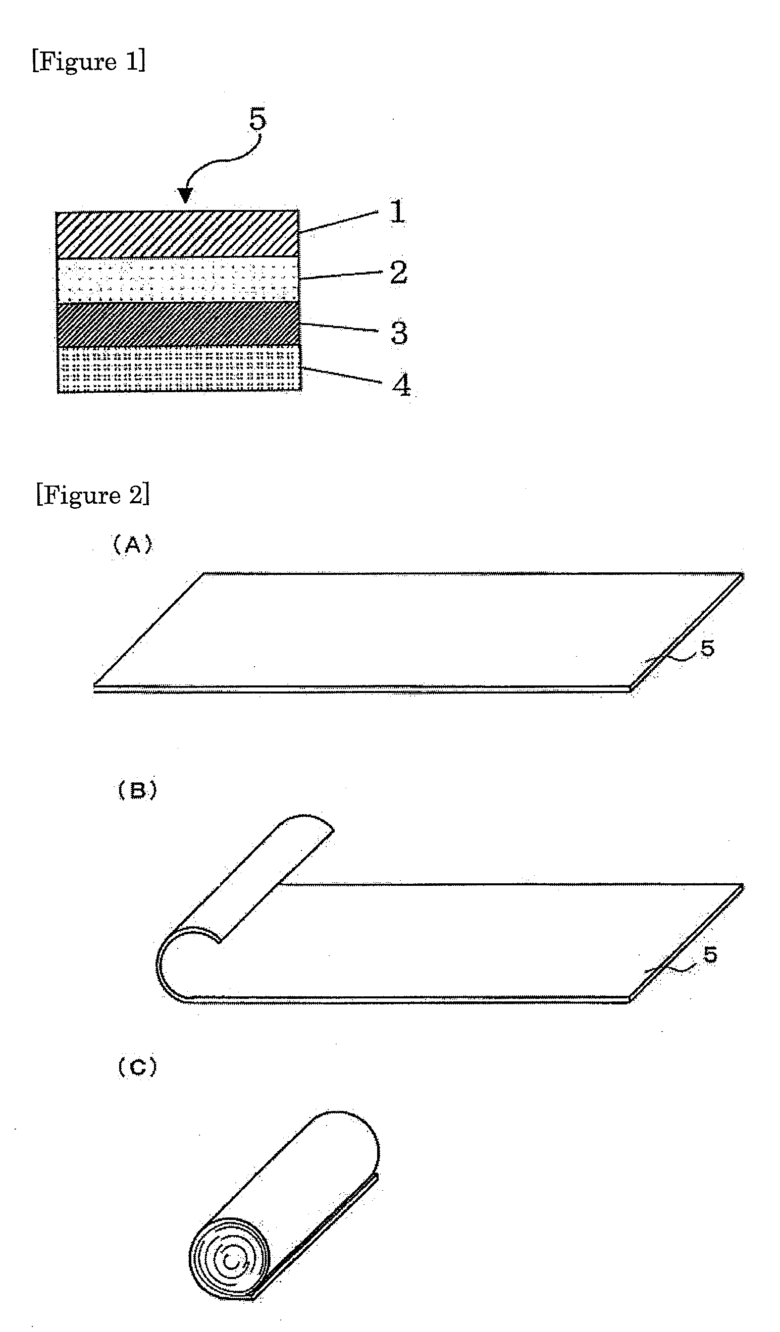
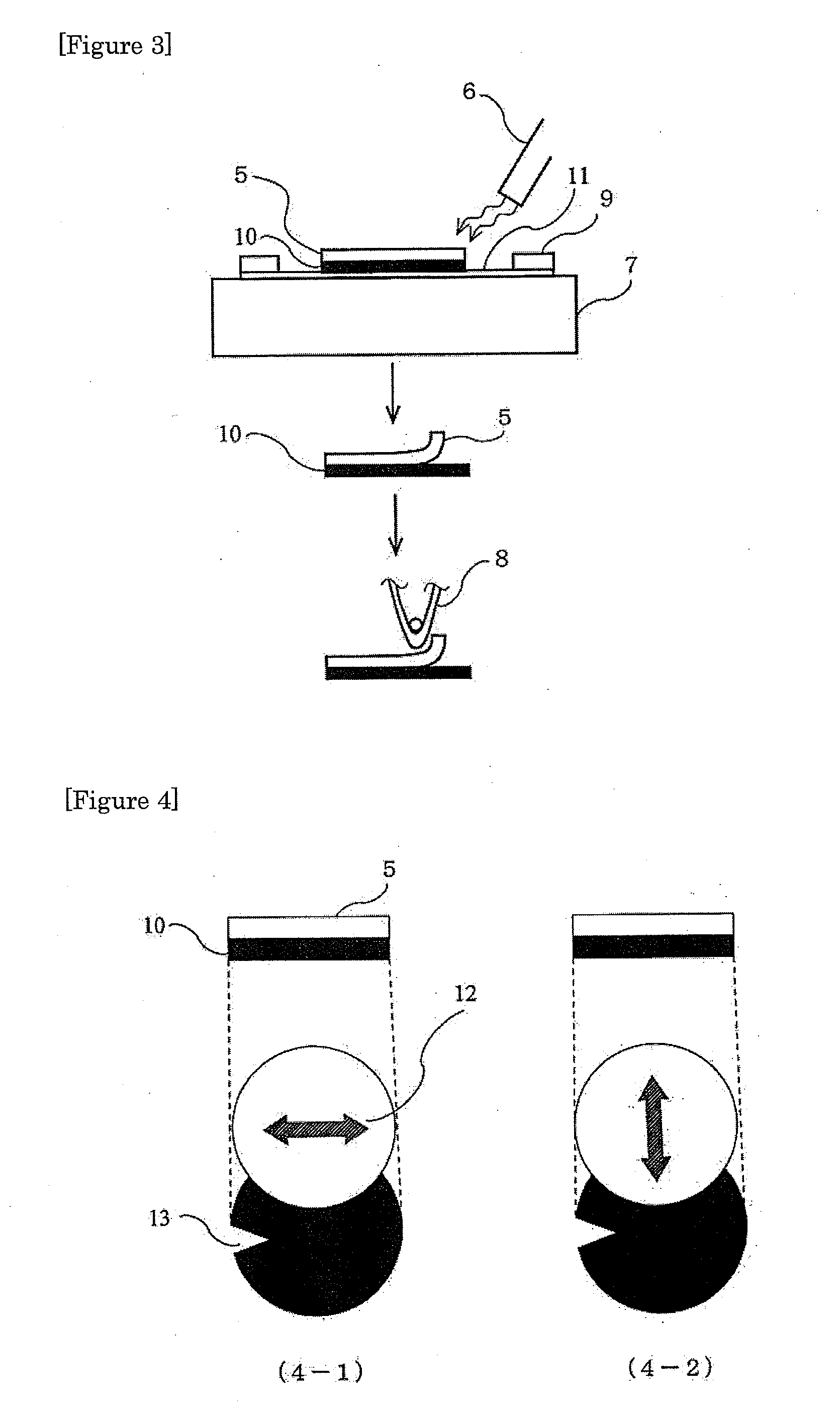
Resin laminate, pressure sensitive adhesive sheet, method for working adherend using the pressure sensitive adhesive sheet, and device for separating the pressure sensitive adhesive sheet
a technology of pressure sensitive adhesives and adhesive sheets, applied in the field of resin laminates, can solve the problems of inability to bond a rectangular release tape to a circumferential, easy fracture of semiconductor wafers, and easy fracture of thin film wafers, and achieve the effect of easily and completely separating the unneeded pressure sensitive adhesive sheets
- Summary
- Abstract
- Description
- Claims
- Application Information
AI Technical Summary
Benefits of technology
Problems solved by technology
Method used
Image

Examples
example 1-1
Preparative Example 1-1
[0097]100 weight parts of an acrylic polymer (trade name: “Leocoat R1020S”, manufactured by Daiichi Lace), 10 weight parts of a pentaerythritol-modified acrylate crosslinking agent (trade name: “DPHA40H”, manufactured by NIPPON KAYAKU Co., Ltd.), 0.25 weight part of a crosslinking agent (trade name: “TETRAD C”, manufactured by MITSUBISHI GAS CHEMICAL COMPANY, INC.), 2 weight parts of a crosslink agent (trade name: “CORONATE L”, manufactured by NIPPON POLYURETHANE INDUSTRY CO., LTD. CO., LTD.), and 3 weight parts of an active energy ray polymerization initiator (trade name: “Irgacure 651”, manufactured by Nihon Ciba-Geigy K.K) were dissolved in toluene to give a polymer solution 1 having a solid matter concentration of 15 weight %. The polymer solution 1 obtained was coated and dried on a polyethylene terephthalate film (trade name: “LUMIRROR S10”, manufactured by Toray Industries Inc., surface-processed PET film for printing, thickness: 38 μm, rigidity at 80° ...
example 1-2
Preparative Example 1-2
[0098]A polymer solution 1 was obtained in a manner similar to the Preparative Example 1-1 above. The polymer solution 1 obtained was coated and dried on a polyethylene terephthalate film (trade name: “LUMIRROR S10”, manufactured by Toray Industries Inc., surface-processed PET film for printing, thickness: 50 μm, rigidity at 80° C.: 1.86×10⁵ N / m) as a low thermally shrinkable base layer to a dried thickness of 30 μm by using a coating machine to form a self-adhesive layer. Then, a biaxially stretched polyester film (trade name: “SPACECLEAN S7200”, manufactured by TOYOBO CO., LTD. CO., LTD., thickness: 30 μm, ratio (A:B) of the shrinkage ratio in the main shrinkage direction [A (%)] to the shrinkage ratio in the direction perpendicular to the main shrinkage direction [B (%)]: 40:40) was laminated on the self-adhesive layer as a high thermally shrinkable base layer to give a resin laminate 2.
example 1-3
Preparative Example 1-3
[0099]100 weight parts of an acrylic polymer: 2-ethylhexyl acrylate / acrylic acid (90 weight parts / 10 weight parts) copolymer, 10 weight parts of dipentaerythritol hexaacrylate and 3 weight parts of an active energy ray polymerization initiator (trade name: “Irgacure 651”, manufactured by Nihon Ciba-Geigy K.K.) were dissolved in toluene to give a polymer solution 2 having a solid matter concentration of 15 weight %. The polymer solution 2 obtained was coated and dried on a polyethylene terephthalate film (trade name: “LUMIRROR S10”, manufactured by Toray Industries Inc., surface-processed PET film for printing, thickness: 38 μm, rigidity at 80° C.: 1.41×10⁵ N / m) as a low thermally shrinkable base layer to a dried thickness of 30 μm by using a coating machine, to form a self-adhesive layer. Then, a biaxially stretched polyester film (trade name: “SPACECLEAN S7200”, manufactured by TOYOBO CO., LTD. CO., LTD., thickness: 30 μm, ratio (A:B) of the shrinkage ratio i...
PUM
| Property | Measurement | Unit |
|---|---|---|
| temperature | aaaaa | aaaaa |
| heat shrinkage ratio | aaaaa | aaaaa |
| rigidity | aaaaa | aaaaa |
Abstract
Description
Claims
Application Information