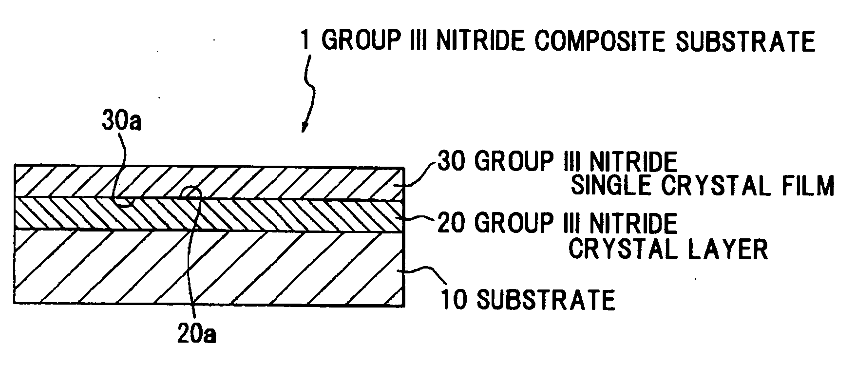
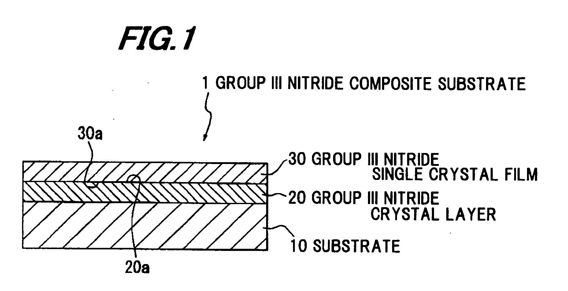
Group III nitride semiconductor composite substrate, group III nitride semiconductor substrate, and group III nitride semiconductor composite substrate manufacturing method
a technology of nitride and semiconductor composite substrates, which is applied in the direction of polycrystalline material growth, crystal growth process, after-treatment details, etc., can solve the problems of voids achieve good electrical conduction and thermal conduction at the laminated interface, reduce the occurrence of voids, and high quality
- Summary
- Abstract
- Description
- Claims
- Application Information
AI Technical Summary
Benefits of technology
Problems solved by technology
Method used
Image

Examples
example 1
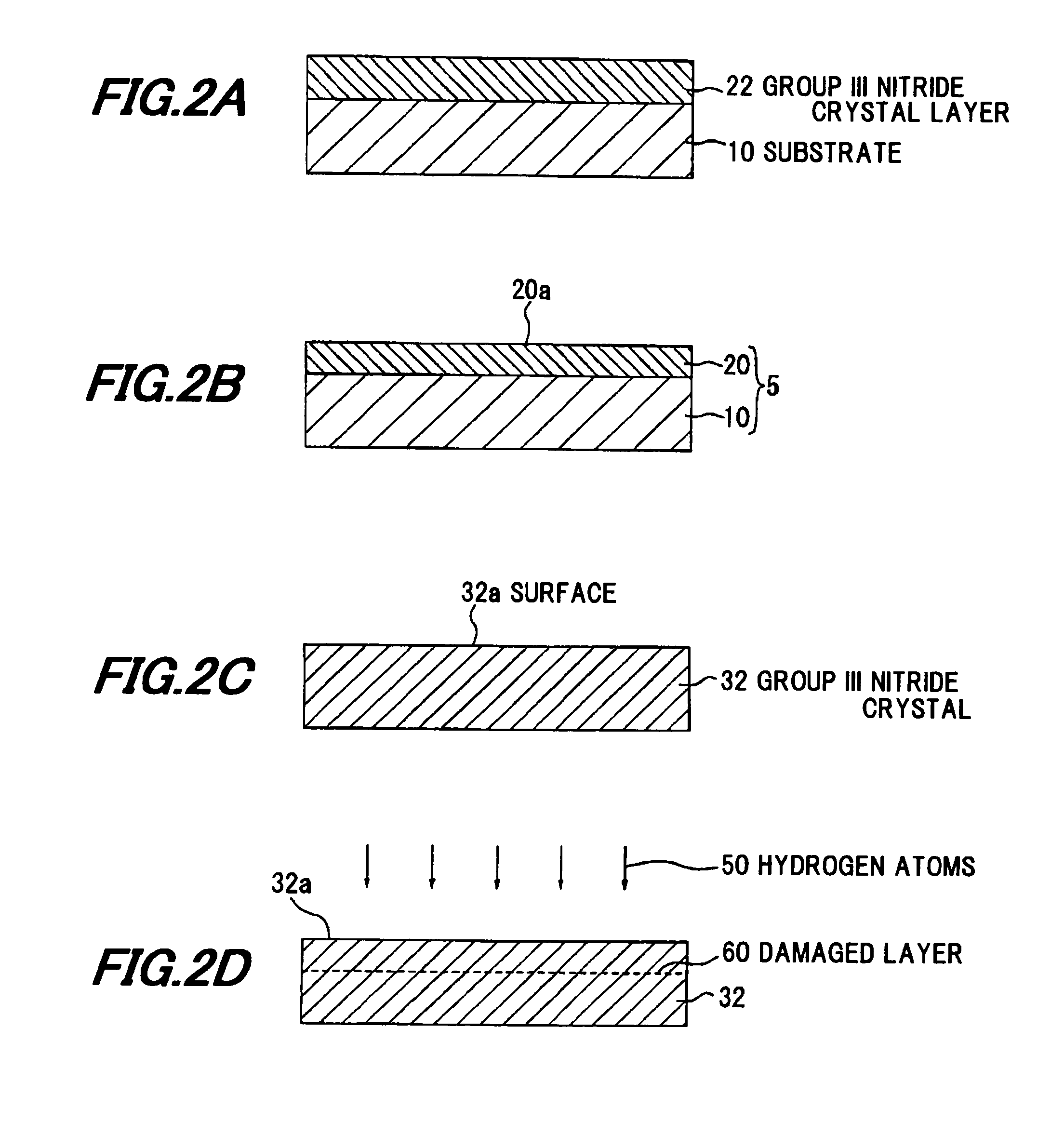
[0088]Group III nitride composite substrate 1 in Example 1 is fabricated based on the manufacturing method explained in the embodiment as follows: First, using HVPE, a 100 μm-thick GaN polycrystalline layer is deposited on a 2-inch diameter molybdenum substrate. Here, the reverse surface Ra of the molybdenum substrate is ground to be 3 μm. Subsequently, the polycrystalline layer deposited is mirror-ground to be 10 μm thick. This results in the substrate with the group III nitride crystal layer in Example 1.
[0089]Here, the grinding conditions are as follows: First, using a wax with a viscosity of 60 cp at 100° C., the wax-coating step is implemented. In the work-fixing step following the wax-coating step, the temperature of laminating the work to a lamination plate is set at 100° C. Here, the work is fixed to the lamination plate at the pressure of 3 kgf / cm2. The lamination plate used has 10 μm surface Ra. A tin surface plate is used in the grinding step.
[0090]Power spectral density ...
example 2
[0102]Etching is done on split surface of the GaN single crystal (i.e., separation layer) separated in Example 1. The etching uses a mixture of phosphoric acid and sulfuric acid (composition 1:1) at 230° C. as an etchant, and is implemented for 1 hour. AFM evaluation is done of power spectral density of the etched split surface. As shown by (f) in FIG. 4, its results are that the power spectral density is 307 (nm3) at the spatial frequency of 0.1 ( / μm), the power spectral density is 72.0 (nm3) at the spatial frequency of 1.0 ( / μm), and the power spectral density is 1.73 (nm3) at the spatial frequency of 12.8 ( / μm), for example.
[0103]This is followed by implanting a hydrogen atom dose of 3×1017 cm2 at 50 keV at room temperature into the etched split surface. Subsequently, the surface of a substrate with a group III nitride crystal layer provided with a GaN layer on molybdenum substrate 10 prepared in the same manner as in Example 1 and the etched split surface of the GaN single cryst...
example 3
[0104]A 2 inch-diameter and 5 mm-thick GaN single crystal (specifically, a single crystal whose crystalline axis in its thickness direction is the c-axis) is prepared, and the Ga-polar face of this GaN single crystal is ground in the following grinding conditions: First, using a wax with a viscosity of 60 cp at 100° C., the wax-coating step is implemented. In the work-fixing step following the wax-coating step, the temperature of laminating the work to a lamination plate is set at 100° C. Here, the work is fixed to the lamination plate at the pressure of 3 kgf / cm2. The reverse surface Ra of the molybdenum substrate used is 3 μm thick, and the surface Ra of the lamination plate used are 10 μm thick. A tin surface plate is used in the grinding step.
[0105]Subsequently, power spectral density analysis using AFM is done in a 10 μm×10 μm range of the ground surface. As shown by (g) in FIG. 4, its results are that the power spectral density is 499 (nm3) at the spatial frequency of 0.1 ( / μm...
PUM
| Property | Measurement | Unit |
|---|---|---|
| melting point | aaaaa | aaaaa |
| surface roughness | aaaaa | aaaaa |
| surface roughness | aaaaa | aaaaa |
Abstract
Description
Claims
Application Information
PatSnap Eureka turns technology decisions into work you can execute. Powered by our Innovation Knowledge Graph, it runs expert workflows across engineering, life sciences, materials and intellectual property. Get your review-ready output in minutes.


