Actuator device for optical deflector

Active Publication Date: 2010-09-30
STANLEY ELECTRIC CO LTD
View PDF8 Cites 71 Cited by
  • Summary
  • Abstract
  • Description
  • Claims
  • Application Information

AI Technical Summary

Benefits of technology

[0029]According to this aspect, the reflected light from an optical deflector mounted on a base which is translated and vibrated by a piezoelectric actuator transmits through the optical window and is modulated. Due to the translation and vibration of the optical deflector and also the modulation of light, coherence between adjac

Problems solved by technology

However, when using a laser beam source as a light source, there is a problem in that speckle noise (granular interference pattern) is generated, resulting in the deterioration of the quality of an image.
Speckle noise is a phenomenon that occurs when a coherent light having a constant phase from a laser beam source is scattered by a random phase plane (object plane), resulting in an interference of a disturbed wave front from adjacent regions of the object plane on an observation plane.
According to the proje

Method used


Image

  • Actuator device for optical deflector
  • Actuator device for optical deflector
  • Actuator device for optical deflector

Examples


first embodiment

[0043]With reference to FIGS. 1 to 6L, a first embodiment of the present invention is described.

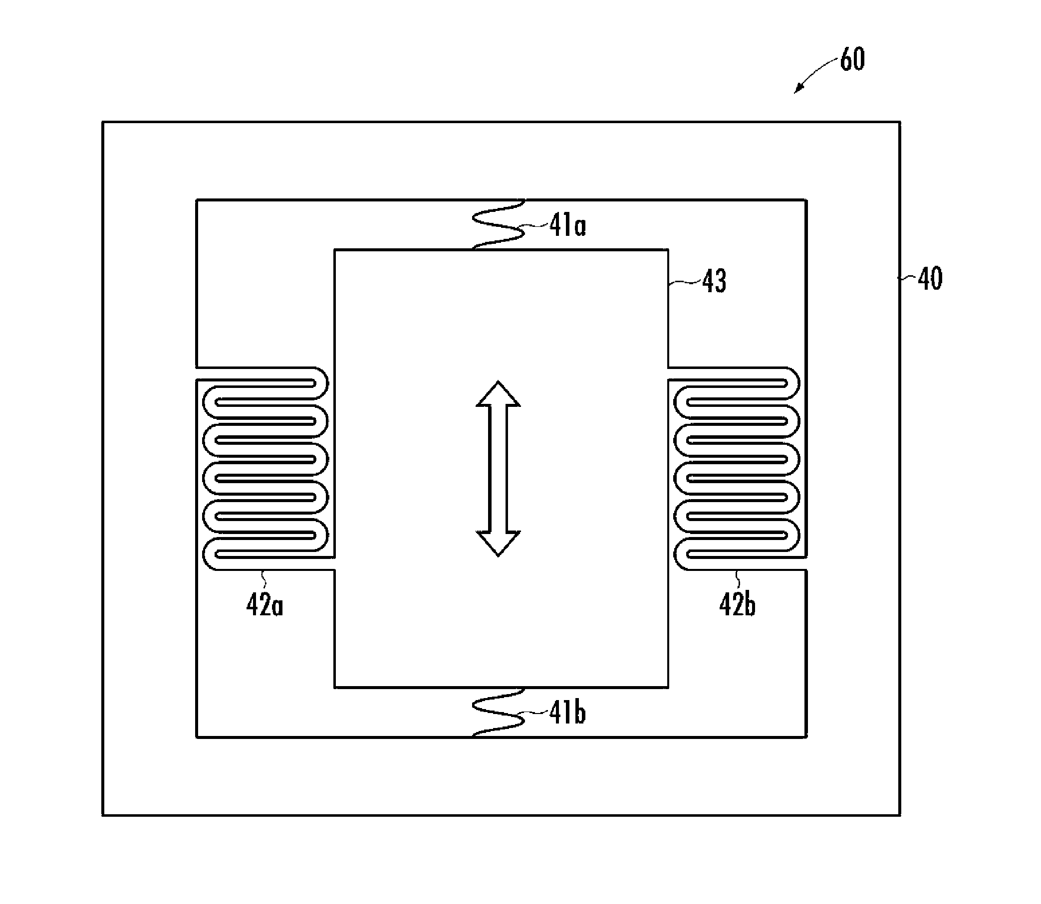
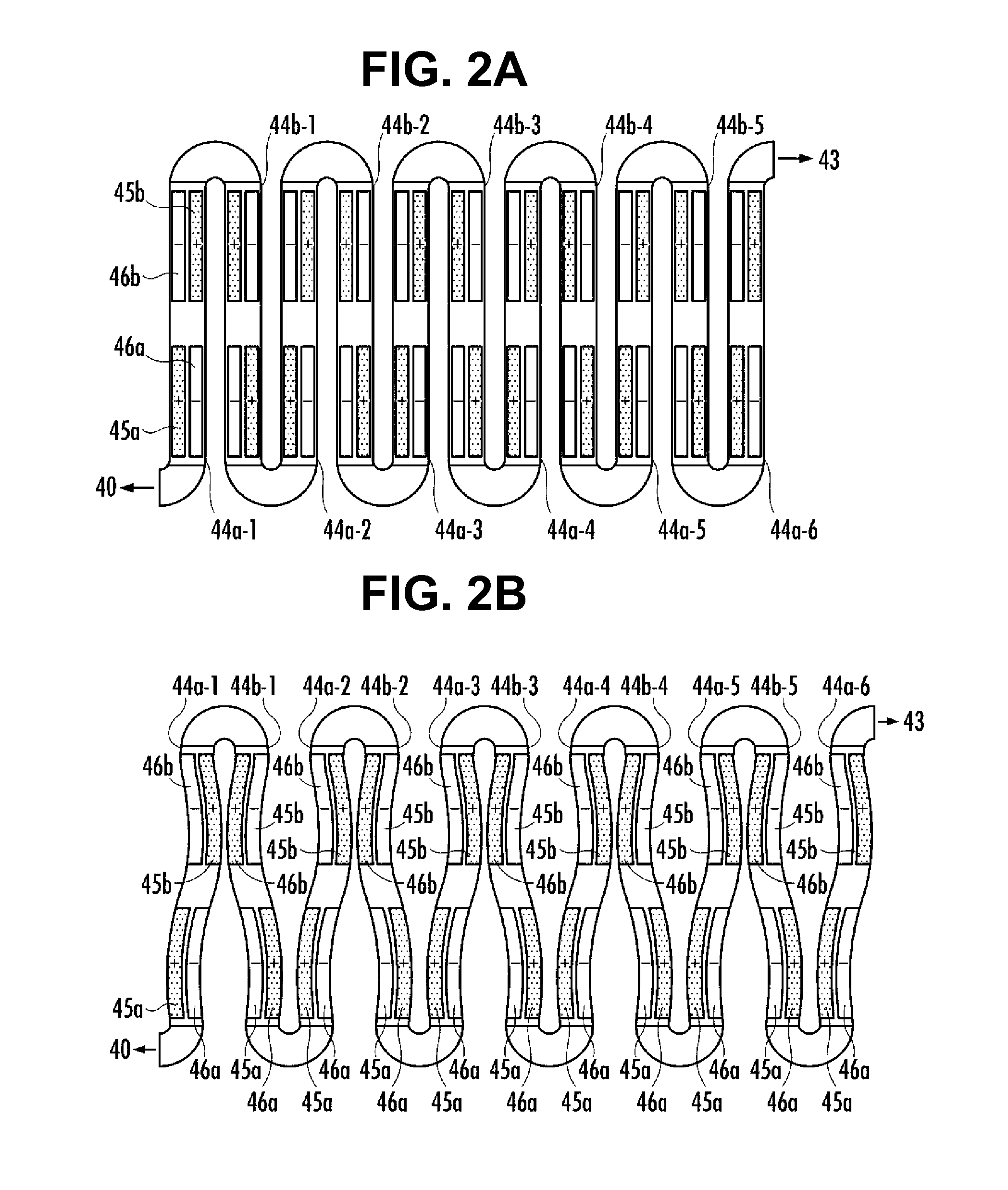
[0044]As shown inFIG. 1, an actuator device for optical deflector 60 of the present embodiment is equipped with a base 43 on which an optical deflector deflecting light from a light source is mounted, one pair of dampers 41a, 41b that support the base 43, piezoelectric actuators 42a, 42b that drive (translate and vibrate) the base 43 as described later, and a supporting body 40 that supports the dampers 41a, 41b and the piezoelectric actuators 42a, 42b.

[0045]The supporting body 40, the dampers 41a, 41b, the piezoelectric actuators 42a, 42b, and the base 43 are integrally formed, for example, by forming a thin film of lead zirconate titanate (PZT), which is a piezoelectric body, on a semiconductor substrate using an ion plating technique or sputtering, followed by performing dry etching on the PZT thin film and the silicon structure of the semiconductor substrate using a semiconductor pla...

second embodiment

[0097]With reference to FIGS. 7 to 11, a second embodiment of the present invention is described.

[0098]As shown in FIG. 7, according to the present embodiment, an actuator device for optical deflector 60 is mounted on a package 72 by securing the optical deflector 71 on the base 43. On the top of the package 72, a transparent optical window 70 is formed to introduce incident light to a reflecting film 1b on the mirror plane of a mirror 1 of the optical deflector 71 shown in FIG. 8.

[0099]The optical deflector 71 may be secured on the base 43 using a bonding system, such as adhesive resin, Au—Sn eutectic bonding, Au—Au solid phase diffusion bonding, solder joint, bump bonding, or the like. In this example, it is secured on the base 43 of the actuator for optical deflector 60 using Au—Au solid phase diffusion bonding.

[0100]In this case, by sputtering Ti, Ni, and Au in this order, a film of each metal material is formed both on the bottom side of the optical deflector 71 and on the base...

working example 1

[0142]As a working example 1, the actuator for optical deflector 60 of the present embodiment, in which the optical deflector 71 was secured on the base 43, was mounted on the package and was tested for its drive characteristics. For the present working example, the thickness of the SOI substrate of the actuator for optical deflector 60 was set to 50 μm for the active layer, 2 μm for the thickness of the interlayer oxide film layer, and 525 μm for the thickness of the handling layer, respectively, and the thickness of the thermally-oxidized silicon film was 500 nm. Also, the thickness of the lower electrode layer (Ti / Pt) was set to 50 nm for Ti and 150 nm for Pt, while the thickness of the piezoelectric layer was 3 μm and that of the upper electrode layer (Pt) was 150 nm.

[0143]Also, in the present working example, the aforementioned optical deflector 71 was designed to have a resonant frequency at 15 kHz. In this optical deflector, an alternating-current voltage of an amplitude volt...


PUM


Abstract

An actuator device for optical deflector includes a base for mounting an optical deflector deflecting a light beam from a light source, at least one piezoelectric actuator translating and vibrating said base; and a supporting body supporting said piezoelectric actuator.

Description

[0001]This application hereby incorporates by reference U.S. Pat. Nos. 7,605,965 and 7,605,966, both issued on Oct. 20, 2009, in their entireties.BACKGROUND OF THE INVENTION[0002]1. Field of the Invention[0003]The present invention relates to an actuator device for optical deflector, on which an optical deflector for deflecting and scanning a light beam such as a laser beam is mounted.[0004]2. Description of the Related Art[0005]Recently, as one form of an image display device, a projection display has been proposed in which a light beam from a light source is deflected by an optical deflector and is projected onto a screen on which an image is displayed. For the optical deflector, for example, an optical deflector in which a mirror, a piezoelectric actuator and other mechanism elements are integrally formed on a semiconductor substrate has been proposed as a MEMS (micro electro mechanical systems) device using semiconductor processes or micro machine technology (see Patent Document...

Claims


Application Information

Patent Timeline
IPC IPC(8): G02B26/08
CPCH01L41/0953G02B26/0858H10N30/2044
Inventor YASUDA, YOSHIAKI
Owner STANLEY ELECTRIC CO LTD
Why Eureka
Try Eureka