Organic electroluminescence device

Inactive Publication Date: 2010-10-07
SEIKO EPSON CORP
View PDF10 Cites 42 Cited by
  • Summary
  • Abstract
  • Description
  • Claims
  • Application Information

AI Technical Summary

Benefits of technology

[0008]An advantage of some aspect of the invention is that it prov

Problems solved by technology

Such a sealing layer, however, has such an internal stress as cracks the ends of the pixel partition layer, and consequently causes moisture penetration.
However, an ex

Method used


Image

  • Organic electroluminescence device
  • Organic electroluminescence device
  • Organic electroluminescence device

Examples


first embodiment

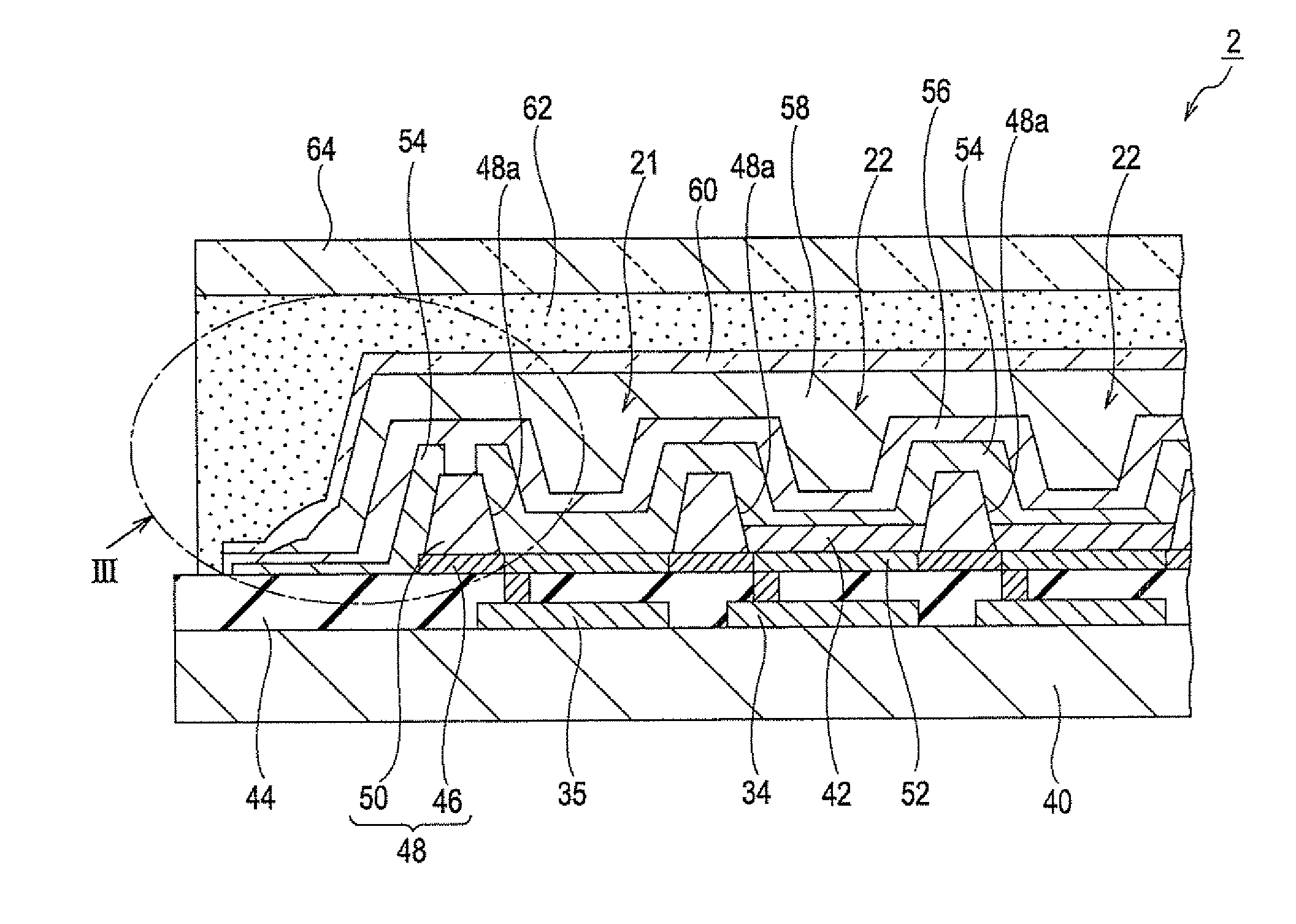
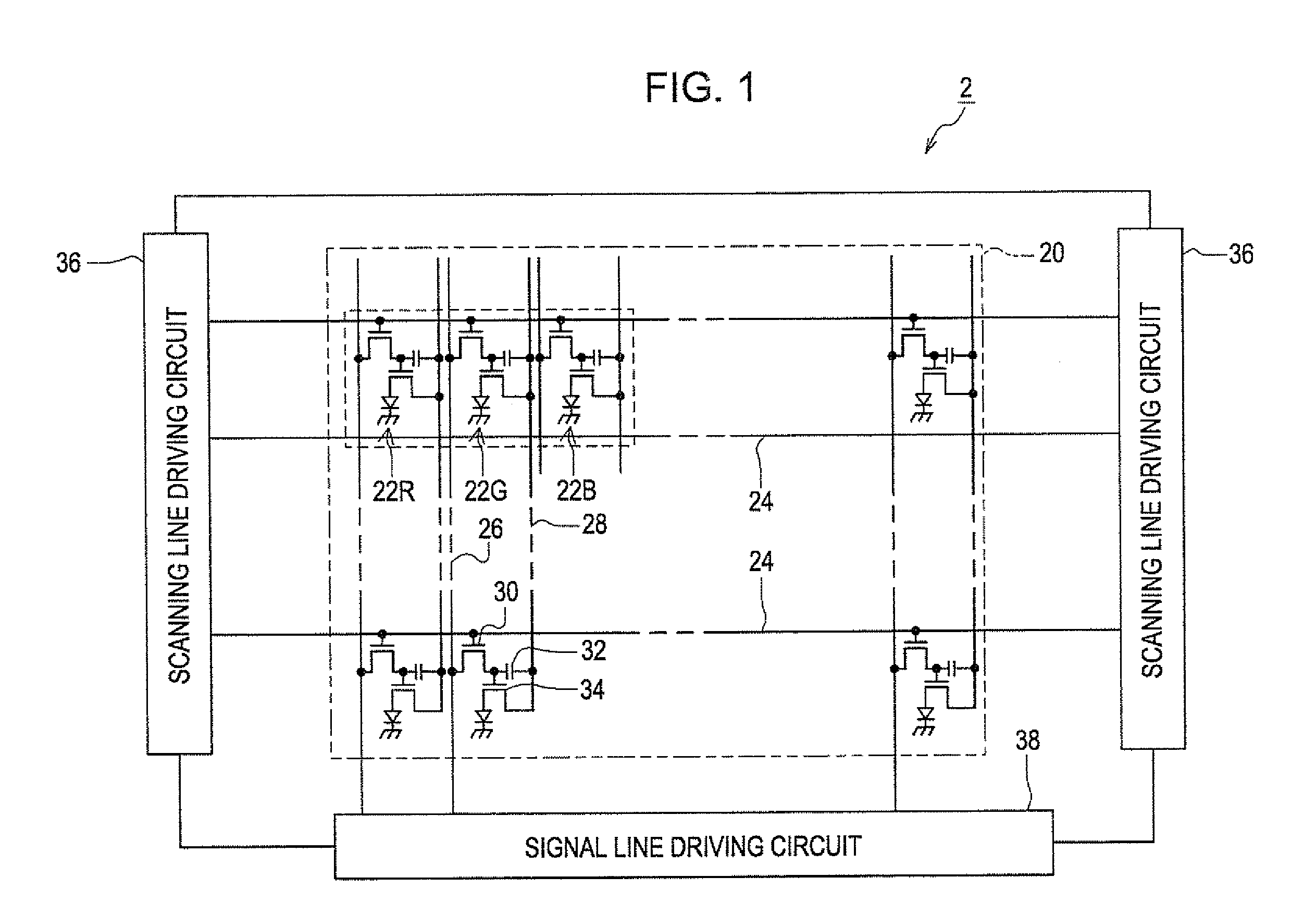
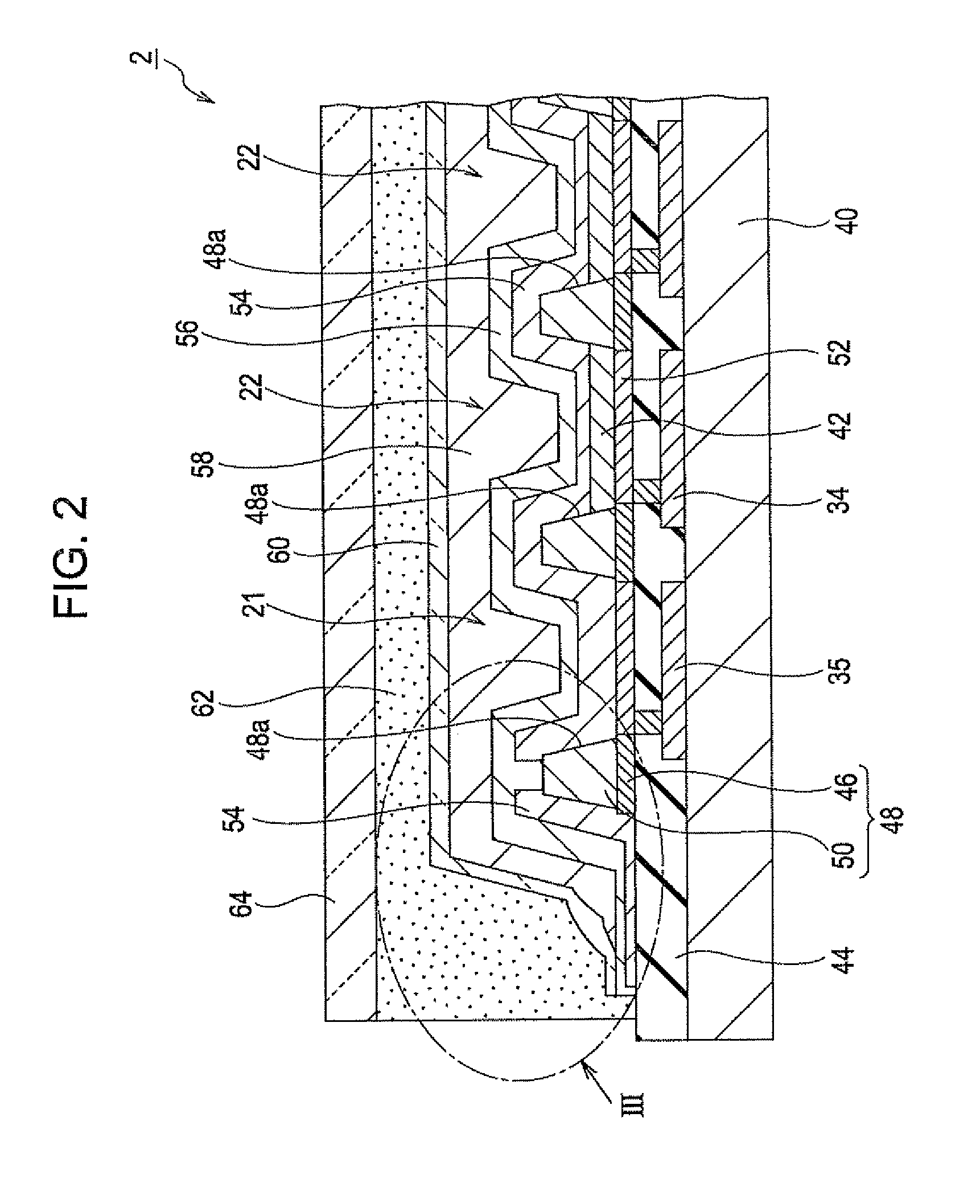
[0039]FIG. 1 is an equivalent circuit diagram of an organic EL device 2 according to a first embodiment of the invention. The organic EL device 2 has a display region 20 including red organic EL elements 22R emitting red light, green organic EL elements 22G emitting green light, and blue organic EL elements 22B emitting blue light. These three types of organic EL elements 22 are regularly arranged in the display region. When it is not required that the color of the emitted light be discriminated, each color organic EL element 22 is referred to as simply organic EL element. The three types of organic EL elements 22 are substantially the same except for the organic EL material used as an electrooptic material.

[0040]The organic EL device 2 is of an active matrix type forming images in the display region 20 including many organic EL elements 22 by controlling light emission of each organic EL element 22. The display region 20 also includes a plurality of scanning lines 24, a plurality o...

second embodiment

[0079]The organic EL device according to a second embodiment includes the organic buffer layer having the same structure as the common cathode layer in the first embodiment. The organic EL device of the second embodiment is a full color display panel using a low-molecular-weight organic EL material described below, and includes organic EL elements emitting white light and color filters for displaying full color images.

[0080]FIG. 8 is a schematic sectional view of an organic EL device 4 according to the second embodiment, and FIG. 9 is a fragmentary enlarged sectional view of portion IX in FIG. 8. The organic EL device 4 includes a flat substrate 72. The substrate 72 may be made of glass or plastic, and a plurality of organic EL elements 74 are disposed on the surface of the substrate 40. Each organic EL element 74 emits white light and includes an organic luminescent layer 76 containing a low-molecular-weight organic EL material described below. The organic luminescent layer 79 rece...

third embodiment

[0099]An organic EL device according to a third embodiment of the present invention is the same as the organic EL device 2 of the first embodiment except for the structure of the organic buffer layer.

[0100]FIG. 10 is a fragmentary enlarged sectional view of an organic EL device 6 according to the third embodiment. The organic EL device 6 of the present embodiment has a first organic buffer layer 102 formed on the cathode protection layer 56 so as to overlie all the organic EL elements 22. The first organic buffer layer 102 thus planarize the unevenness formed by the presence of the partition structure 48. A second organic buffer layer 104 is formed on the first organic buffer layer 102 so as to overlie all the organic EL elements 22. A gas barrier layer 60 is formed over the cathode protection layer 56, the first organic buffer layer 102 and the second organic buffer layer 104 to fully cover the entirety of the first and second organic buffer layers 102 and 104 including their ends....


PUM


Abstract

An organic electroluminescence device includes on a substrate a plurality of first electrodes, a partition structure having a plurality of openings corresponding to the positions of the first electrodes, an organic luminescent layer, a second electrode covering the partition structure and the organic luminescent layer, and a sealing layer or a sealing member covering the second electrode. The second electrode includes a first portion and a second portion that are separate from each other. The first portion covers the entire partition structure except the outer portion from the edge of the partition structure, and the organic luminescent layer. The second portion covers the outer portion from the edge of the partition structure and at least part of the external region around the partition structure.

Description

BACKGROUND[0001]1. Technical Field[0002]The present invention relates to an organic electroluminescence device (hereinafter referred to as organic EL device).[0003]2. Related Art[0004]A known organic EL device includes an organic EL element disposed on, for example, a glass substrate. The organic EL element includes a pair of electrodes and a multilayer composite disposed between the electrodes and including an organic luminescent layer (light-emitting layer made of an organic material). For sealing the organic EL device, a glass plate may be disposed over the multilayer composite with an epoxy adhesive applied therebetween. The adhesive is cured to act as a sealing layer.[0005]In general, an inorganic sealing layer is formed to cover the entire surface of a pixel partition layer. The inorganic sealing layer can be formed by sputtering or chemical vapor deposition (CVD). From the viewpoint of enhancing the moisture resistance, it is preferable that the inorganic sealing layer be den...

Claims


Application Information

Patent Timeline
IPC IPC(8): H01L51/54
CPCH01L27/3246H01L2251/5315H01L51/5237H01L51/5234H10K59/122H10K50/828H10K50/846H10K50/8426H10K2102/3026H10K50/844H10K59/12H10K50/822H10K50/84
Inventor FUKAGAWA, TAKEFUMINISHIOKA, DAISUKE
Owner SEIKO EPSON CORP
Why Eureka
Try Eureka