Nonvolatile latch circuit and logic circuit using the same

a logic circuit and latch circuit technology, applied in the direction of magnetic field-controlled resistors, digital storage, instruments, etc., can solve the problems of increasing operating power due to speed increase affecting the reliability of logic circuits, etc., and achieve high reliability and efficient holding

Active Publication Date: 2010-10-21
NEC CORP
View PDF6 Cites 16 Cited by
  • Summary
  • Abstract
  • Description
  • Claims
  • Application Information

AI Technical Summary

Benefits of technology

[0015]An object of the present invention is to provide a nonvolatile latch circuit using a magnetoresistance element, in which even after power supply has been stoppe...

Problems solved by technology

Along with this, an increase in operating power due to an increase in speed, and an increase in standby power represented by a leak current become problems.
However, this method causes an initial data, intermediate process data, result data, or the like to disappear.
This causes power supply control to be complicated, and a component cost in a system to be increased.
Also, at the time of a power failure due to lightening, or an instantaneous power failure due to an unforeseen accident or the like, the procedure for transferring the processing data may not be appropriately performed.
Further, in a latch circuit or a flip-flop circuit, an initial data is arbitrary, and therefore an initializing operation of a logic circuit is required at the time of power-on, which is disadvantageous in that system activation is delayed.
Also, three power supply lines,...

Method used


Image

  • Nonvolatile latch circuit and logic circuit using the same
  • Nonvolatile latch circuit and logic circuit using the same
  • Nonvolatile latch circuit and logic circuit using the same

Examples


first embodiment

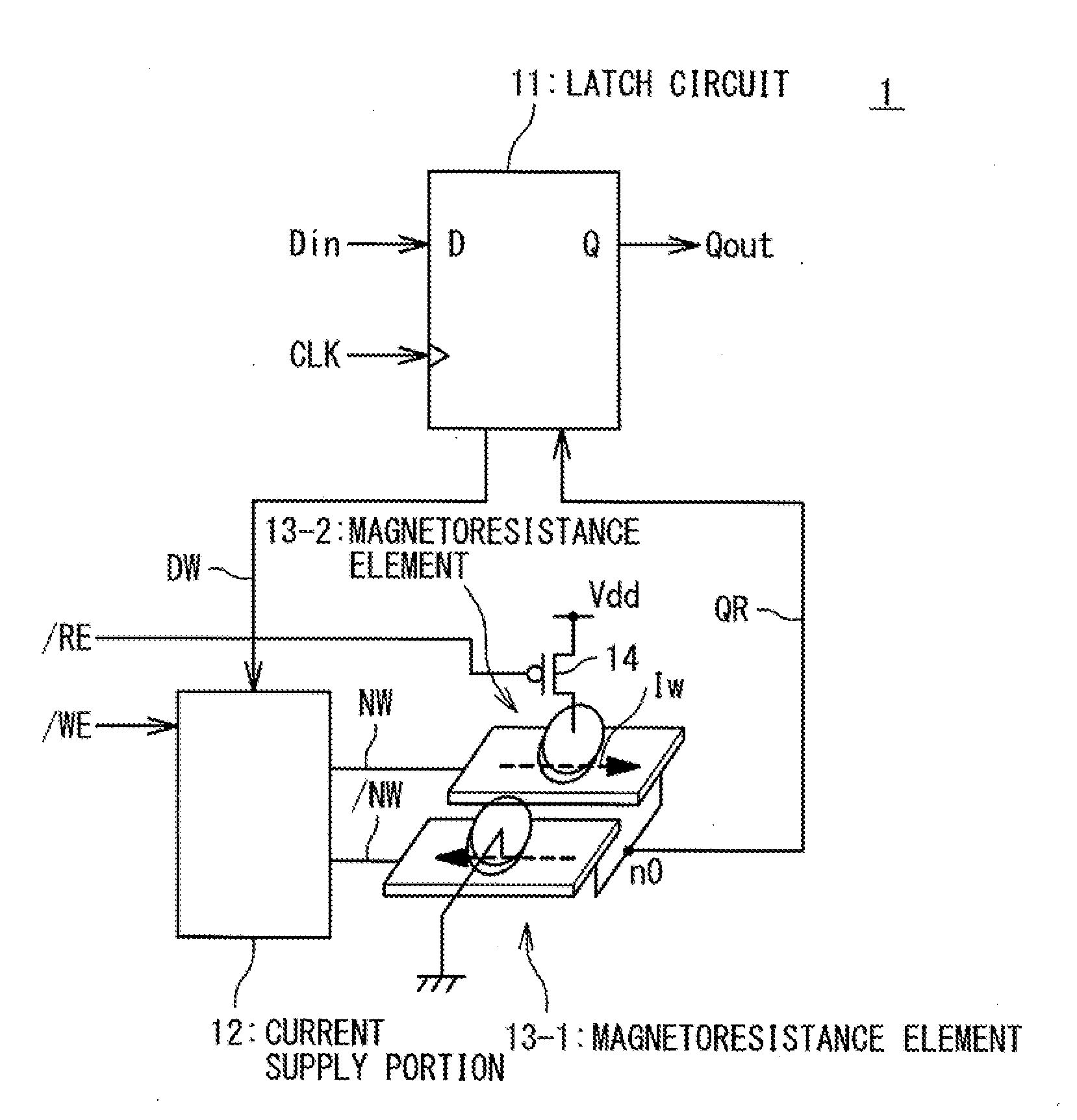
[0045]A configuration of a nonvolatile latch circuit according to a first embodiment of the present invention will be described. FIG. 1 is a schematic configuration diagram illustrating the configuration of the nonvolatile latch circuit according to the first embodiment of the present invention. The nonvolatile latch circuit 1 is a nonvolatile latch circuit using a magnetoresistance element exemplified by an MTJ element. The nonvolatile latch circuit 1 includes a latch circuit 11, two magnetoresistance elements 13-1 and 13-2, and a current supply portion 12.

[0046]During a time period that a clock signal CLK is at a high level (or a low level), the latch circuit 11 temporarily holds (latches) input data Din supplied from another circuit (not illustrated) within a logic circuit. Then, the latch circuit 11 outputs the latched data (latch data) as output data Qout. Also, the latch circuit 11 supplies a data signal DW (or an inverted signal / DW of the data signal DW) indicating the latch...

second embodiment

[0094]An example in which a nonvolatile latch circuit using a magnetoresistance element is applied to a delay flip-flop (DFF) will be described as the nonvolatile latch circuit of the present invention. FIG. 10 is a schematic configuration diagram illustrating a configuration of a nonvolatile latch circuit according to a second embodiment of the present invention. The nonvolatile latch circuit 1b uses, in the delay flip-flop of a master-slave system, as a slave latch, a circuit equivalent to the high through latch circuit (nonvolatile latch circuit 1a) illustrated in FIGS. 5A and 5B. The nonvolatile latch circuit 1b includes a master latch circuit 11-1, a slave latch circuit 11-2, a current supply portion 12, signal conversion portions 16 and 17, a clocked inverter CI15, and magnetoresistance elements 13-1 and 13-2.

[0095]The master latch circuit 11-1 includes clocked inverters CI11 and CI12. The clocked inverter CI11 is supplied with input data Din and clock signals p1 and / p1, and ...

third embodiment

[0110]Another example in which a nonvolatile latch circuit using a magnetoresistance element is applied to a delay flip-flop (DFF) will be described as the nonvolatile latch circuit of the present invention. FIG. 13 is a schematic configuration diagram illustrating a configuration of a nonvolatile latch circuit according to a third embodiment of the present invention. The nonvolatile latch circuit 1c uses, in the delay flip-flop of a master-slave system, the non-volatile low through latch circuit using the magnetoresistance elements based on the first embodiment as a master latch circuit, and the non-volatile high through latch circuit using the magnetoresistance elements based on the first embodiment as a slave latch circuit. The nonvolatile latch circuit 1c is provided with a master latch circuit 11-1a, a clocked inverter CI24, a current supply portion 12-1, magnetoresistance elements 13-11 and 13-21, a slave latch circuit 11-2a, a clocked inverter CI27, a current supply portion 1...


PUM


Abstract

A nonvolatile latch circuit includes: a latch circuit; a first magnetoresistance element and a second magnetoresistance element; and a current supply portion. The latch circuit temporarily holds data. Each of the first magnetoresistance element and the second magnetoresistance element includes a first magnetic layer and a second magnetic layer that are stacked with an insulating film sandwiched therebetween. The current supply portion complementarily changes magnetization states of the first magnetoresistance element and the second magnetoresistance element based on a state of the latch circuit. The first magnetic layer of the first magnetoresistance element and the first magnetic layer of the second magnetoresistance element are series-connected to each other in. The latch circuit has a function that brings data corresponding to the magnetization states to data held by the latch circuit.

Description

TECHNICAL FIELD[0001]The present invention relates to a nonvolatile latch circuit including a magnetoresistance element (MTJ: Magnetic Tunnel Junction) as a memory element, and a logic circuit using the nonvolatile latch circuit.BACKGROUND ART[0002]In a large-scale integrated circuit (LSI), a large number of logic circuits are used. The logic circuits are roughly classified into logic gates and bistable logic circuits. The logic gate is used to process a digital logic value, and represented by an inverter, an NAND gate, or an NOR gate. The bistable logic circuit is used to temporarily hold or store a digital logic value, and represented by any of various types of latch circuits, or any of various types of flip-flop circuits combining them. A typical LSI incorporates large numbers of logic gates and bistable logic circuits, which are combined with each other. In recent years, the LSI often simultaneously incorporates a memory core such as a random access memory (RAM) or a read only m...

Claims


Application Information

Patent Timeline
IPC IPC(8): G11C11/00G11C7/10
CPCG11C11/16H03K3/45H01L43/08H01L27/226G11C11/18G11C11/1659G11C11/161G11C11/1673G11C11/1675G11C11/1693H10B61/20H10N50/10
Inventor SAKIMURA, NOBORUSUGIBAYASHI, TADAHIKONEBASHI, RYUSUKE
Owner NEC CORP
Why Eureka
Try Eureka