Polishing pad for cmp, method for polishing substrate using it and method for producing polishing pad for cmp

a technology of polishing pad and cmp, which is applied in the direction of flexible wheel, manufacturing tools, grinding devices, etc., can solve the problems of insufficient speed of polishing inorganic insulation film, ineffective reduction of polishing flaws, and insufficient hardness of pad surface, so as to suppress the occurrence of polishing flaws

Inactive Publication Date: 2004-11-11
HITACHI CHEM CO LTD +1
View PDF8 Cites 20 Cited by
  • Summary
  • Abstract
  • Description
  • Claims
  • Application Information

AI Technical Summary

Benefits of technology

0005] The present invention provides a polishing pad and a method of polishing a substrate whereby in the CMP technology employed in the production of semiconductor elements for planarizing an interlayer insulation film, a BPSG film, an insulation film for shallow trench isolation, etc., irregularities on a matter to be polished, such as a silicon oxide film, are planarized efficiently at a high speed while suppressing the occurrence of polishing flaws on the substrate. The present invention further provides a method of producing the polishing pad.

Problems solved by technology

A polishing pad made of polyurethane foam has commonly been used in the above-described method, which however is insufficient in the speed of polishing the inorganic insulation film, and involves the great problem that polishing flaws occur during polishing on the surface of the oxide film due to polishing particles.
In the case of a pad made of a foamed or non-foamed resin, decreasing the hardness of the pad surface reduces the polishing flaws effectively, but materials of low hardness do not suit to planarize irregularities efficiently in the production of semiconductor devices.
To solve the problem, pad materials compromising the reduction of polishing flaws and the improvement of flatness are used, but are not enough to solve the problem of polishing flaws.

Method used


Image

  • Polishing pad for cmp, method for polishing substrate using it and method for producing polishing pad for cmp
  • Polishing pad for cmp, method for polishing substrate using it and method for producing polishing pad for cmp

Examples


example 1

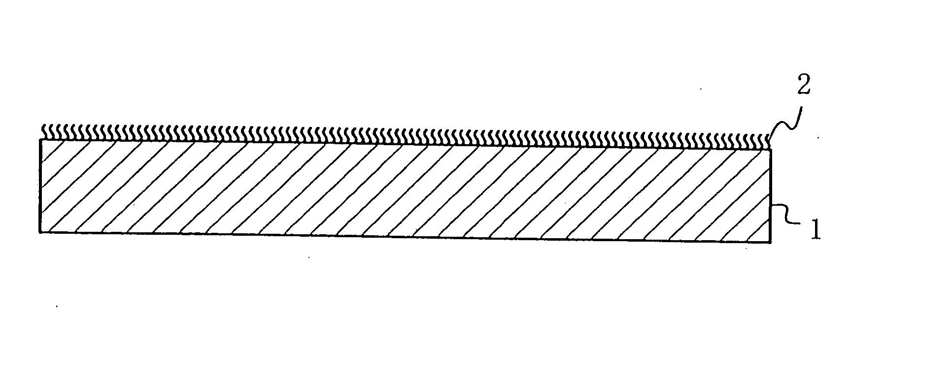
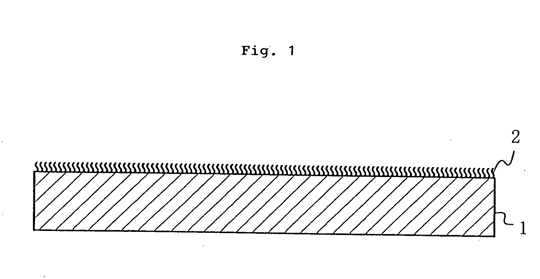
[0061] A release film (a 50.mu.m-thick polypropylene film) was put on both surfaces of a prepreg layer consisting of 15 sheets of prepreg "1," put in layers. They were sandwiched between mirror-finished plates and thermocompression molded (temperature: 175.degree. C., pressure: 400 kPa, time: 120 min.) between pressing hot plates, with two sheets of 10 mm-thick cushion interposed, to give a 1.5 mm-thick laminate. A polishing pad was produced by sticking the laminate to the fixing disc of a polishing machine, and dressing it with a diamond whetstone of #70 count for 10 minutes under a pressure of 8820 Pa (90 g / cm.sup.2) at revolutions of 38 rpm to form a very thin layer of exposed aramid fibers on a surface. The exposed parts of the aramid fibers had a fiber length of 1 mm and a fiber diameter of 12.5.mu.m.

example 2

[0062] A polishing pad was produced by sticking a laminate, which was produced in the same manner as in Example 1, to the fixing disc of a polishing machine, and dressing it with a diamond whetstone of #150 count for 10 minutes under a pressure of 8820 Pa (90 g / cm.sup.2) at revolutions of 38 rpm to form a very thin layer of exposed aramid fibers on a surface. The exposed parts of the aramid fibers were shorter than those of Example 1, and had a fiber length of 500 .mu.m and a fiber diameter of 12.5 .mu.m.

examples 3 to 7

Production of Pad

[0073] The following organic fibers were prepared as raw materials.

[0074] [Polyester Fiber Base Material "1"]

[0075] A non-woven fabric consisting of polyester fibers having a fiber diameter of 12.5.mu.m and a fiber length of 5 mm and having a unit weight of 70 g / m.sup.2 ([EPM-4070TE] produced by Nippon Byleen Co., Ltd.).

[0076] [Aramid fiber base material "2"]

[0077] Para-aramid fiber chops (fiber diameter: 12.5.mu.m, fiber length: 5 mm, "KEVLAR" produced by DuPont Kabushiki Kaisha), para-aramid fiber pulps (fiber diameter: 0.83.mu.m, fiber length: 1 mm, "KEVLAR" produced by DuPont Kabushiki Kaisha) and meta-aramid fiber chops (fiber diameter: 25.mu.m, fiber length: 6 mm, softening temperature: 280.degree. C., "CORNEX" produced by Teijin Ltd.) were mixed and made into a mat. A 20% by weight aqueous solution of a water-soluble epoxy resin binder (glass transition temperature: 110.degree. C., trade name: "V-COAT", produced by Dainippon Ink & Chemicals, Inc.) was sprayed...


PUM

PropertyMeasurementUnit
diameteraaaaaaaaaa
lengthaaaaaaaaaa
lengthaaaaaaaaaa

Abstract

In CMP technology for planarizing an interlayer insulation film, a BPSG film, an insulation film for shallow trench isolation, or the like, in the production process of a semiconductor element, irregularities of a matter being polished, e.g. a silicon oxide film, are planarized efficiently at a high speed while suppressing the occurrence of polishing flaws on the substrate by employing a polishing pad having organic fibers exposed on the surface thereof abutting against the matter being polished.

Description

[0001] The present invention relates to a polishing pad for CMP, which is usable in the chemical mechanical polishing (CMP) method employed in the production technology of semiconductor elements and in the polishing method employed in thee production technology of hard discs. The present invention further relates to a method for polishing a substrate by using the polishing pad and to a method for producing a polishing pad.[0002] In the present ultra large scale integrated circuits, packaging density is increasing, and a variety of fine processing techniques are being studied and developed. Design rule has already been of the order of sub-half-micron. One of the techniques developed to meet the requirement for such a strict miniaturization is the CMP (chemical mechanical polishing) technique. In the production process of semiconductor devices, this technique can completely planarize a layer to be exposed to light, thereby lightening the burden of exposure techniques and stabilizing t...

Claims


Application Information

Patent Timeline
Patent Type & Authority Applications(United States)
IPC IPC(8): B24B37/20B24B37/24B24D11/00B24D13/14B24D18/00H01L21/3105
CPCB24B37/22B24B37/24B24D11/00B24D18/0009H01L21/31053H01L21/304
Inventor NISHIYAMA, MASAYAHABIRO, MASANOBUIWATSUKI, YASUHITOHIRAOKA, HIROKAZU
Owner HITACHI CHEM CO LTD
Why Eureka
Try Eureka