
Integrated coupling structures

a technology of integrated coupling and sensor package, which is applied in the direction of generator/motor, emergency protective arrangement for limiting excess voltage/current, instruments, etc., can solve the problems of complex devices, high cost and complexity, and inability to address the need, etc., to achieve repeatable sensor performance, reduce cost and complexity, and reduce production cost

Inactive Publication Date: 2010-10-28
MICROSEMI CORP HIGH PERFORMANCE TIMING
View PDF7 Cites 15 Cited by
  • Summary
  • Abstract
  • Description
  • Claims
  • Application Information

AI Technical Summary

Benefits of technology

[0007]Benefits of the invention include simple production, repeatable sensor performance, smaller size, enhanced reliability, reduced cost, easier installation, and greater environment immunity.
[0009]In some embodiments, the mutual coupling reactance is large compared to acoustic resistance of the AWD and resistance of the transceiver is large compared to the acoustic resistance, minimizing load perturbations of resonant frequency of the AWD. In another embodiment, the mutual coupling reactance is small compared to acoustic resistance of the AWD and resistance of the transceiver is large compared to the acoustic resistance, minimizing load perturbations of resonant frequency of the AWD. For other embodiments, the package provides mechanical and electromagnetic isolation for operation in hazardous environments. Embodiments include further comprising power dissipative elements providing electrostatic discharge (ESD) protection and series capacitive elements providing electrostatic discharge (ESD) protection. In yet other embodiments, the system operates between about approximately 200 MHz and about approximately 3 GHz. For some embodiments, at least one integrated coupling structure is at least one conductive region and the reactive coupling is capacitively-reactive coupling.

Problems solved by technology

These separate elements lead to added cost and complexity, fabrication difficulties and reliability issues.
Achieving these objectives results in expensive, complex devices and does not address the need for close-coupled, passive-wireless sensors with little or no radiated power and similar applications.
It does not identify solutions with sensor packages that include integrated coupling and sensing components.

Method used


Image

  • Integrated coupling structures
  • Integrated coupling structures
  • Integrated coupling structures

Examples


Embodiment Construction

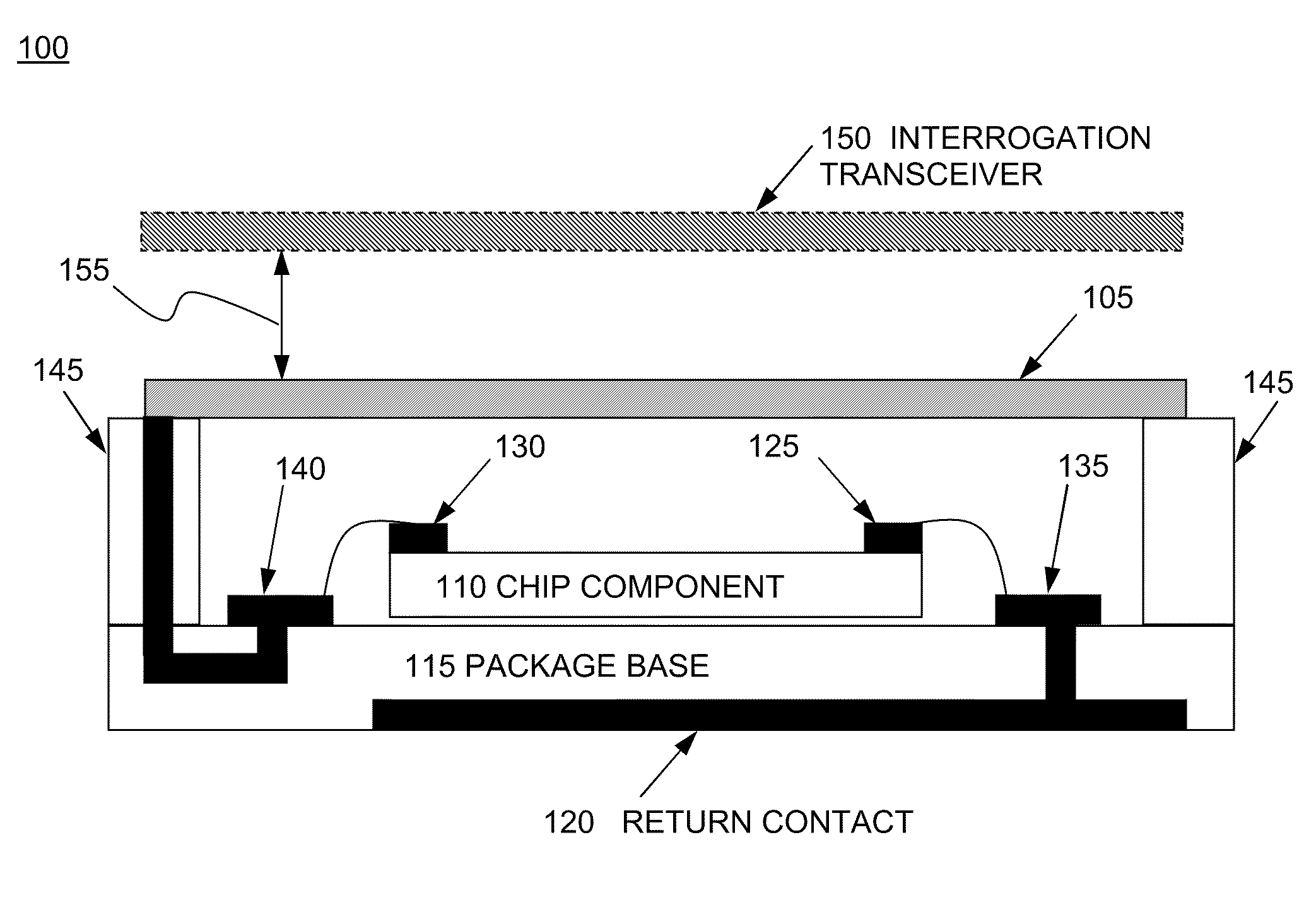
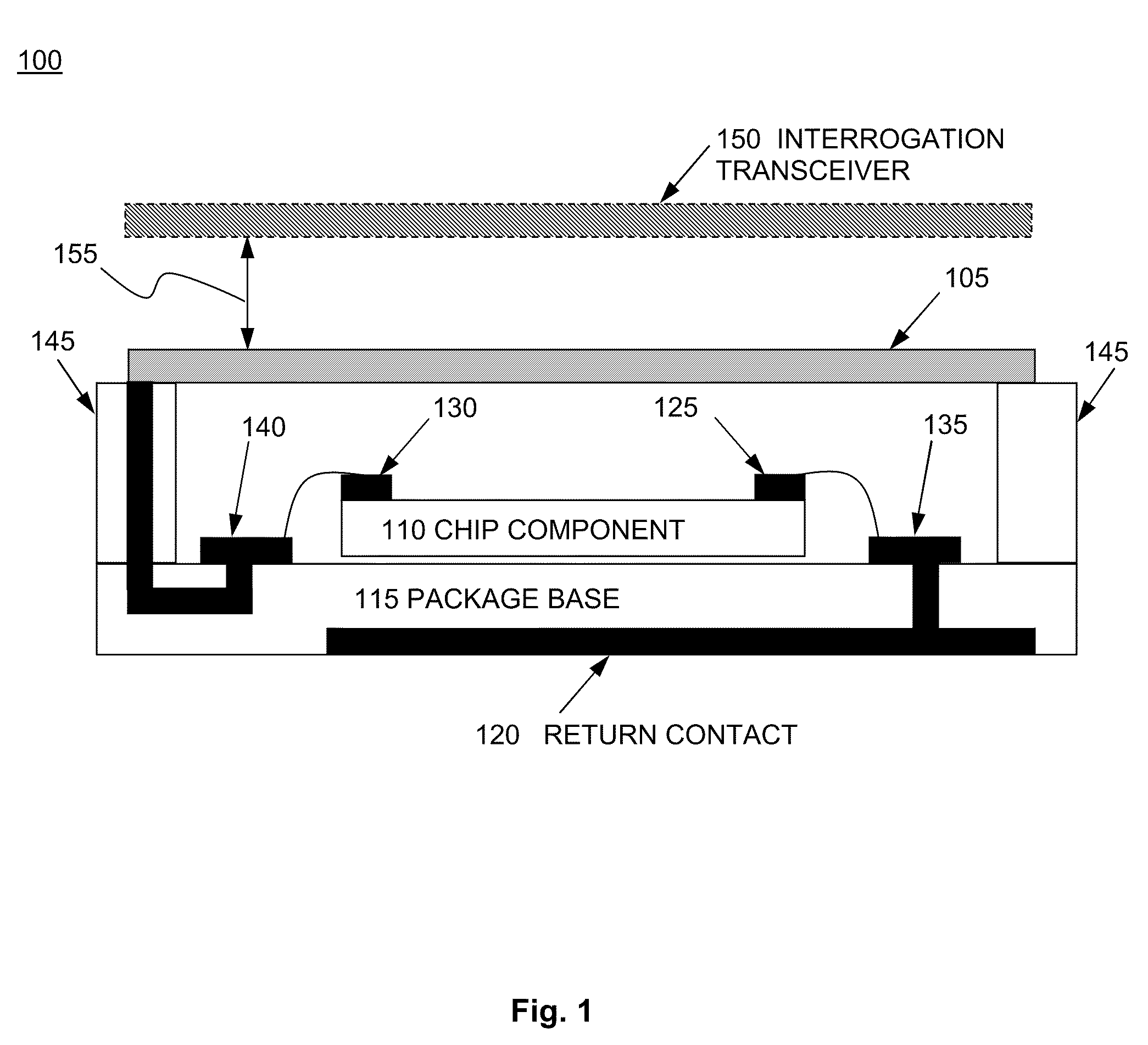
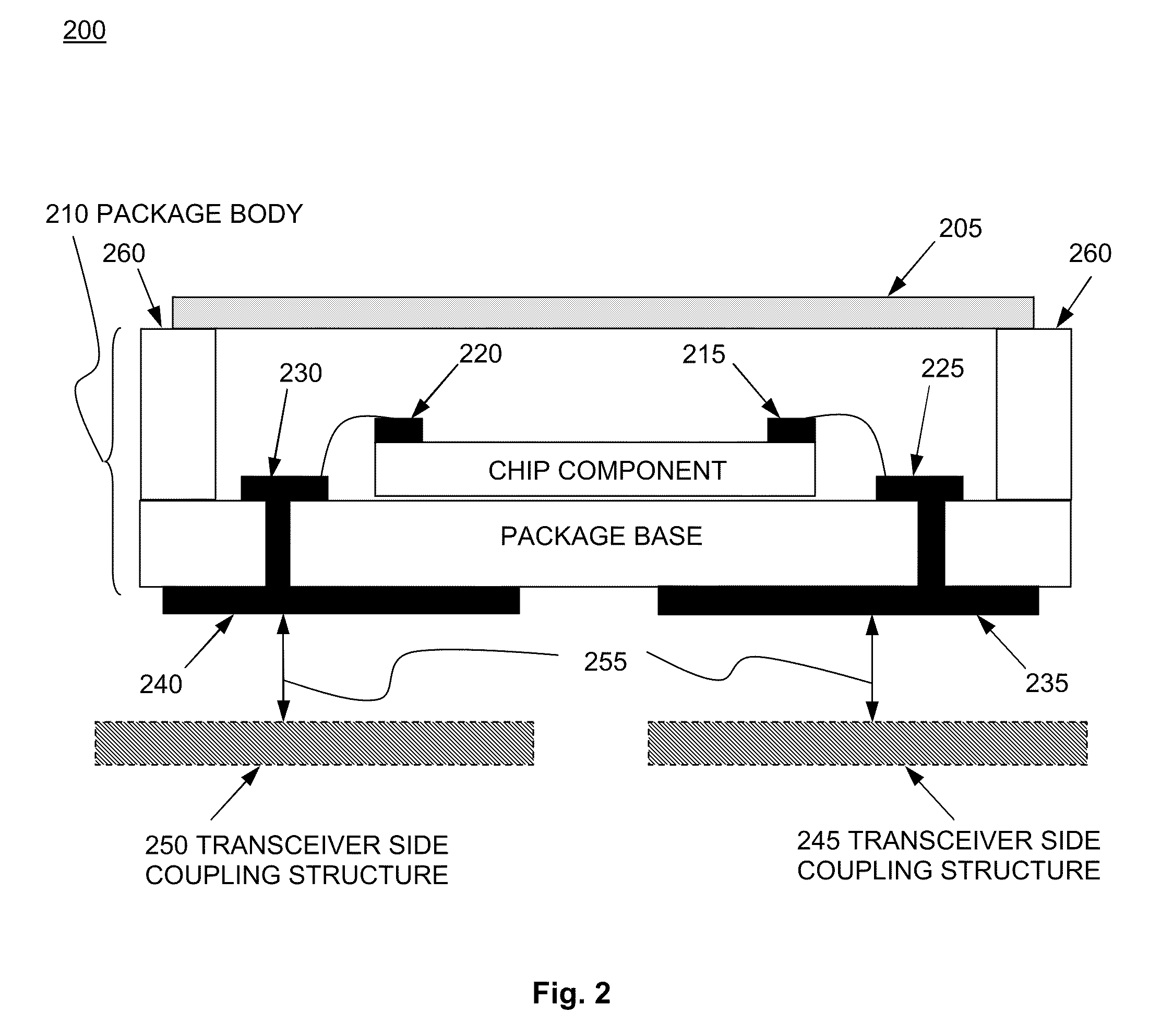
[0033]The invention provides sensor and data transmission capabilities in a single sensor package. A novel Surface Mount Technology (SMT) package with integrated coupling structures for use in near-field, close-coupled, wireless acoustic wave device AWD sensor applications is disclosed. The integrated sensor greatly reduces the size and cost of the transceiver and sensor antennas replacing antennae and mechanical coupling structures with a single package comprising the sensor and associated near field coupling structures. The cost and size of the AWD sensor is dramatically reduced by integrating the AWD sensor chip and the coupling structure within the same package. A reduction in size and the elimination of interconnects and feed lines reduces electromagnetic radiation, simplifying EMC / EMI compliance and reducing the demands of filtering in the transceiver circuit.

Coupling Types

[0034]In addition to far-field propagating wave coupling, there exist near-field coupling applications fo...


PUM


Abstract

An integrated package provides contactless communication through a coupling mechanism embedded in the package. Package types include Surface Mount Technology (SMT), Low Temperature Co-fired Ceramic (LTCC) technology, and dual-in-line integrated circuit pressed ceramic packages generally. The package can include an acoustic wave device (AWD) sensor such as a surface acoustic wave (SAW) device or a bulk acoustic wave (BAW) device. Coupling includes inductive and capacitive effects through plates, loops, spirals, and coils. Coil inductance and SAW capacitance can be parallel resonant at the desired SAW resonance with the coil impedance higher than the SAW impedance, minimizing load-pull effects.

Description

FIELD OF THE INVENTION[0001]The invention relates to wireless sensor packages with integrated coupling structures and, more particularly, embodiments including near-field wireless Acoustic Wave Devices (AWDs) inductively or capacitively coupled to a physically disconnected transceiver.BACKGROUND OF THE INVENTION[0002]Existing SAW devices have been used in a variety of fluid, physical and chemical sensors. Features of SAW sensors include an ability to operate without an external power-supply and an ability to be interrogated wirelessly. Wireless sensor communication systems involve multiple components including sensor, antenna and interconnections. These separate elements lead to added cost and complexity, fabrication difficulties and reliability issues.[0003]Some Antenna-in-Package (AiP) devices are known as in “Novel Antenna-in-Package Design in LTCC for Single-Chip RF Transceivers”, Zhang, Y. P.; Sun, M.; Lin, W.; Antennas and Propagation, IEEE Transactions, Volume 56, Issue 7, Ju...

Claims


Application Information

Patent Timeline
IPC IPC(8): H03H9/76H03H9/48H02H9/00
CPCG01L19/083
Inventor SABAH, SABAHANDLE, JEFFREY CSTEVENS, DANIEL S
Owner MICROSEMI CORP HIGH PERFORMANCE TIMING
Learn More