

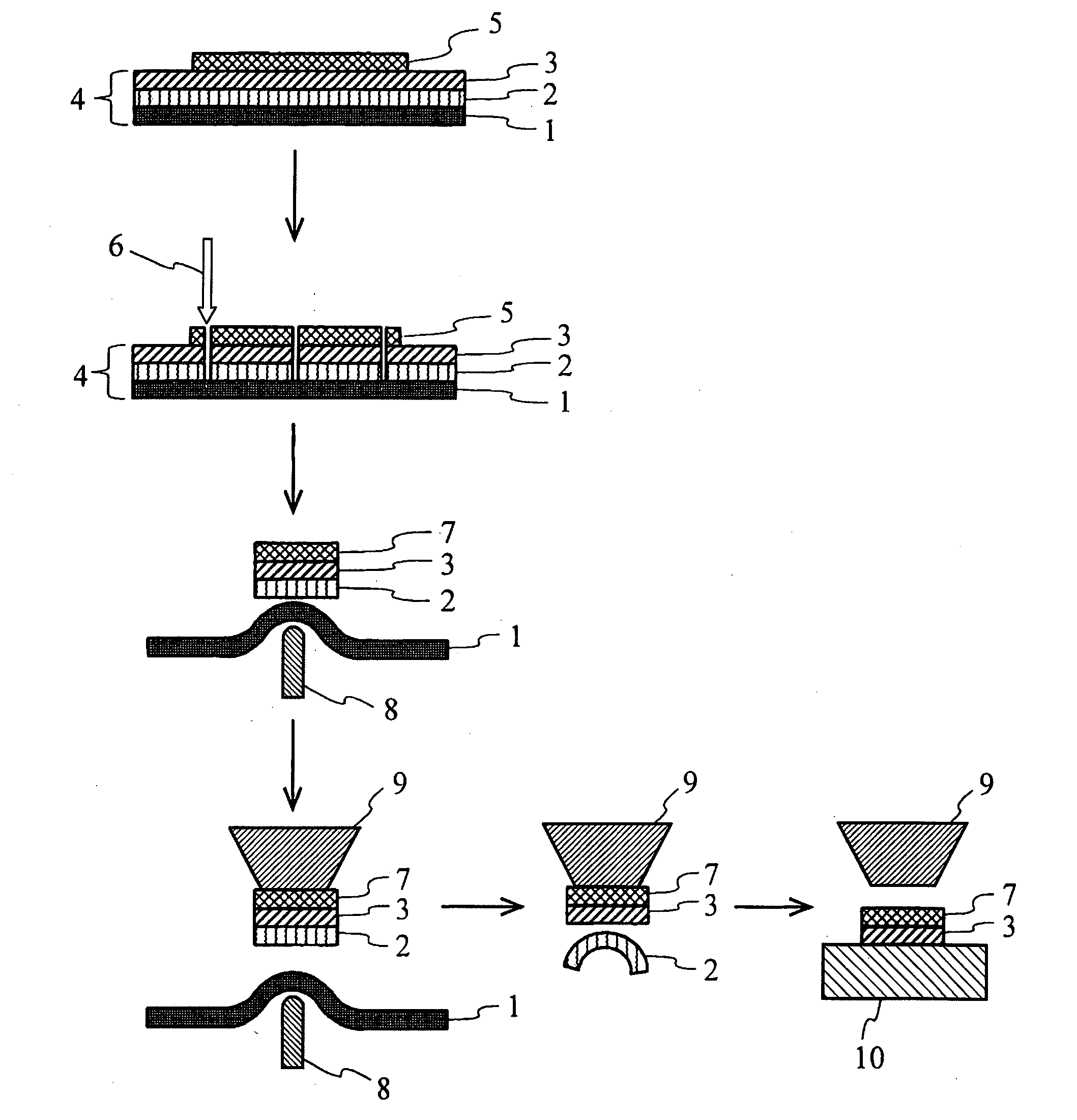
Die attach film-provided dicing tape and production process of semiconductor device
a technology of film-provided dicing tape and production process, which is applied in the direction of adhesive articles, solid-state devices, synthetic resin layered products, etc., can solve the problems of reducing the success rate of die-attaching picking and the mounting efficiency is not reduced, so as to achieve convenient removal, reduce the rate of success of picking, and reduce the effect of production cos
- Summary
- Abstract
- Description
- Claims
- Application Information
AI Technical Summary
Benefits of technology
Problems solved by technology
Method used
Image

Examples
production example 1
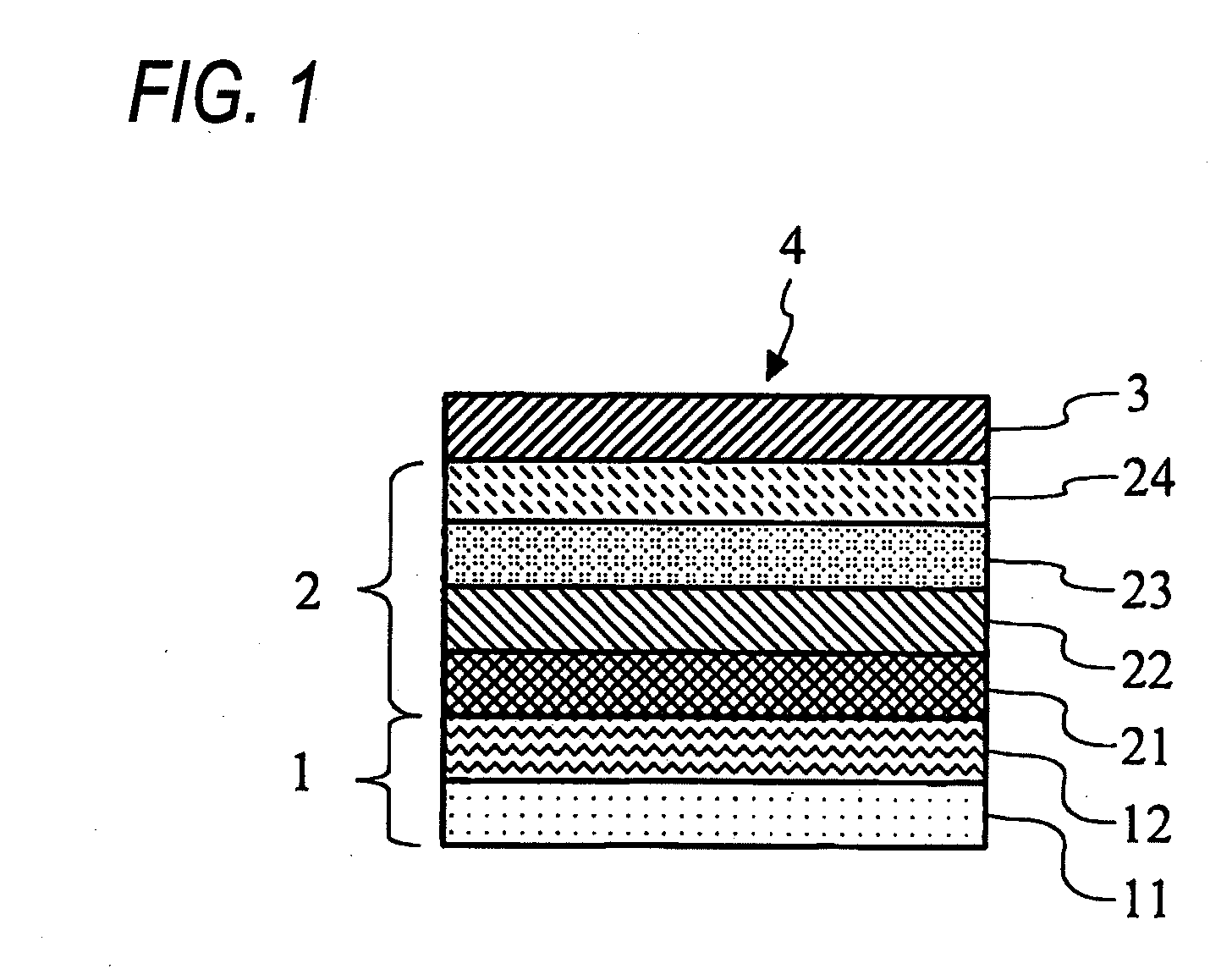
Production of Die Attach Film
[0165]Based on 100 parts by weight of an acrylic acid ester-based polymer mainly composed of ethyl acrylate-methyl methacrylate (“PARACRON W-197CM”, trade name, produced by Negami Chemical Industrial Co., Ltd.), 59 parts by weight of an epoxy resin (“EPIKOTE 1004”, produced by JER), 53 parts by weight of an epoxy resin (“EPIKOTE 827”, trade name, produced by JER), 121 parts by weight of a phenolic resin (“MILEX XLC-4L”, trade name, produced by Mitsui Chemicals, Inc.) and 222 parts by weight of spherical silica (“SO-25R”, trade name, produced by Admatechs Co., Ltd.) were dissolved in methyl ethyl ketone to prepare an adhesive composition solution having a solid content concentration of 23.6 wt %. The obtained adhesive composition solution was coated on a PET film (thickness: 38 μm) release-treated with silicone as a release liner (separator), and then dried at 130° C. for 2 minutes to produce a 20 μm-thick die attach film.
production example 2-1
Production of Pressure-Sensitive Adhesive Layer
[0166]Based on 100 parts by weight of an acrylic copolymer (obtained by copolymerizing 2-ethylhexyl acrylate / morpholyl acrylate / acrylic acid / 2-hydroxyethyl acrylate=75 / 25 / 3 / 0.1 (by weight)], 2 parts by weight of a crosslinking agent (“TETRAD-C”, trade name, produced by Mitsubishi Gas Chemical Industries Ltd.), 2 parts by weight of a crosslinking agent (“Coronate L”, trade name, produced by Nippon Polyurethane Industry Co., Ltd.) and 0.05 parts by weight of “EPAN 710” (trade name, produced by Daiichi Kogyo Seiyaku Co., Ltd.) were mixed to prepare a pressure-sensitive adhesive (non-active energy ray-curable pressure-sensitive adhesive).
[0167]The obtained pressure-sensitive adhesive was coated on a release sheet (“MRF38”, trade name, produced by Mitsubishi Polyester Film Corp.) by using an applicator, and volatiles such as solvent were dried to obtain a 30 μm-thick pressure-sensitive adhesive layer.
production example 2-2
Production of Active Energy Ray-Curable Pressure-Sensitive Adhesive Layer
[0168]An acrylic polymer having a methacrylate group in the side chain was produced by bonding 60% of 2-hydroxyethyl acrylate-derived hydroxyl group in an acrylic polymer [composition: obtained by copolymerizing 2-ethylhexyl acrylate / morpholyl acrylate / 2-hydroxyethyl acrylate=70 / 30 / 20 (by weight)] to methacryloyloxyethyl isocyanate (2-isocyanatoethyl methacrylate). Based on 100 parts by weight of the acrylic polymer having a methacrylate group in the side chain, 50 parts by weight of a compound containing two or more functional groups having a carbon-carbon double bond (“SHIKO UV1700”, trade name, produced by The Nippon Synthetic Chemical Industry Co., Ltd.), 3 parts by weight of photoinitiator (“IRGACURE 184”, trade name, produced by Ciba Japan) and 3.5 parts by weight of crosslinking agent (“Coronate L”, trade name, produced by Nippon Polyurethane Industry Co., Ltd.) were mixed to prepare an energy ray-curabl...
PUM
| Property | Measurement | Unit |
|---|---|---|
| Time | aaaaa | aaaaa |
| Time | aaaaa | aaaaa |
| Height | aaaaa | aaaaa |
Abstract
Description
Claims
Application Information