Methods for tailoring the surface topography of a nanocrystalline or amorphous metal or alloy and articles formed by such methods

a technology of amorphous metals and nanocrystalline metals, applied in the manufacture of printed circuits, electrolysis components, manufacturing tools, etc., can solve problems such as the formation of pits on chromium films

Inactive Publication Date: 2010-11-11
MASSACHUSETTS INST OF TECH
View PDF13 Cites 29 Cited by
  • Summary
  • Abstract
  • Description
  • Claims
  • Application Information

AI Technical Summary

Benefits of technology

[0125]A closely related embodiment of an invention hereof, further comprises using a low deposition duty cycle to obtain a surface exhibiting a plurality of spaced apart pits. Using a low deposition duty cycle with a high etching duty cycle, achieves a plurality of pits that are wide, or de

Problems solved by technology

The regions of the chromium film that are not covered by the sleeve

Method used


Image

  • Methods for tailoring the surface topography of a nanocrystalline or amorphous metal or alloy and articles formed by such methods
  • Methods for tailoring the surface topography of a nanocrystalline or amorphous metal or alloy and articles formed by such methods
  • Methods for tailoring the surface topography of a nanocrystalline or amorphous metal or alloy and articles formed by such methods

Examples


example

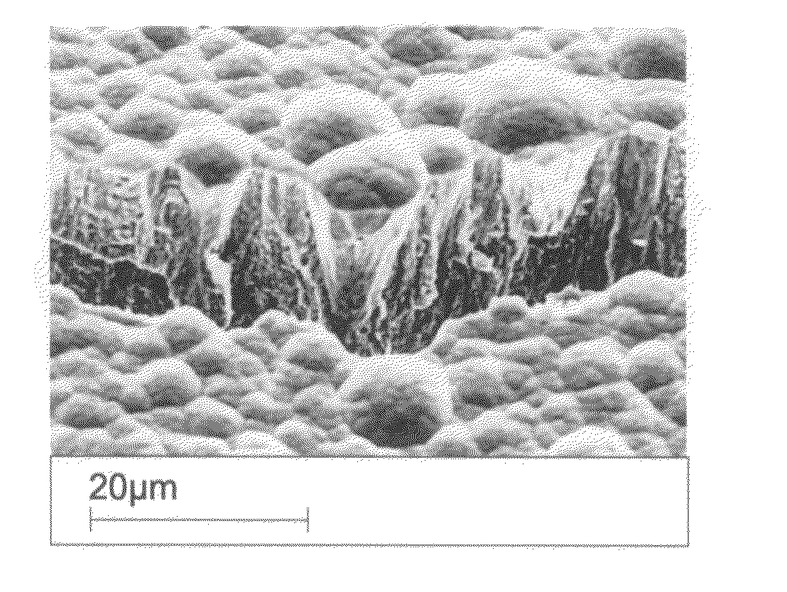
[0031]The use of etching methods to establish the surface morphology of nanocrystalline or amorphous metals or alloys has been reduced to practice for a particular case of a binary alloy of nickel-tungsten. Of the many existing methods that can be used to produce nanocrystalline or amorphous metals or alloys, electrochemical deposition has been used successfully. The electrochemically deposited nanocrystalline nickel-tungsten alloy is etched by a galvanostatic electrochemical etching method.

Electrochemical Deposition

[0032]The composition of the electrolytic bath, which is maintained at approximately 76° C., is shown in Table 1. The cathode and anode used for electrochemical deposition are a copper substrate and platinum electrode respectively.

TABLE 1Composition of electrolytic bathNickel sulfate hexahydrate (NiSO4•6H2O)0.06 MSodium tungstate hexahydrate (Na2WO4•2H2O)0.14 MSodium citrate dihydrate (Na3C6H5O7•2H2O) 0.5 MAmmonium chloride (NH4Cl) 0.5 M

[0033]Traditional electrochemical ...


PUM

PropertyMeasurementUnit
Current densityaaaaaaaaaa
Thicknessaaaaaaaaaa
Diameteraaaaaaaaaa

Abstract

Electrochemical etching tailors topography of a nanocrystalline or amorphous metal or alloy, which may be produced by any method including, by electrochemical deposition. Common etching methods can be used. Topography can be controlled by varying parameters that produce the item or the etching parameters or both. The nanocrystalline article has a surface comprising at least two elements, at least one of which is metal, and one of which is more electrochemically active than the others. The active element has a definite spatial distribution in the workpiece, which bears a predecessor spatial relationship to the specified topography. Etching removes a portion of the active element preferentially, to achieve the specified topography. Control is possible regarding: roughness, color, particularly along a spectrum from silver through grey to black, reflectivity and the presence, distribution and number density of pits and channels, as well as their depth, width, size. Processing parameters that have been correlated in the Ni—W system to topography features include, for both the deposition phase and the etching phase of a nanocrystalline surface: duty cycle, current density, deposition duration, plating chemistry, polarity ratio. The relative influence of the processing parameters can be noted and correlated to establish a relationship between values for processing parameters and degree of topography feature. Control can be established over the topography features. Correlation can be made for any such system that exhibits a definite spatial distribution of an active element that bears a predecessor spatial relationship to a desired topography feature.

Description

RELATED DOCUMENTS[0001]The benefit of U.S. Provisional application No. 60 / 859,067, filed on Nov. 15, 2006, is hereby claimed, and its entire disclosure is hereby incorporated fully herein, by reference.INTRODUCTION[0002]Metals and alloys with nanocrystalline or amorphous structures often exhibit superior physical and / or functional properties, such as high strength, high corrosion-resistance and low coefficient of friction. They may also have desirable magnetic, electronic, optical, or biological properties in specific applications. For these reasons, nanocrystalline or amorphous metals and alloys are gaining wide usage throughout many industries.[0003]Nanocrystalline metal refers to a metallic body in which the number-average size of the crystalline grains is less than one micrometer. The number-average size of the crystalline grains provides equal statistical weight to each grain. The number-average size of the crystalline grains is calculated as the sum of all spherical equivalent...

Claims


Application Information

Patent Timeline
IPC IPC(8): C25D5/10C25F3/02C25D5/48
CPCB23H9/008C25D5/18C25F3/14C25F3/08C25D5/48C25D5/605C25D5/611C25D5/617C25D5/619C25D5/627
Inventor SCHUH, CHRISTOPHER A.RUAN, SHIYUN
Owner MASSACHUSETTS INST OF TECH
Why Eureka
Try Eureka