Process for the deposition of uniform layer of particulate material
a technology of particulate material and uniform layer, applied in the field of deposition technologies, can solve the problems of inherently difficult control of highly dynamic operative processes, limited material class, and inability to process materials with ress based thin film technology, and achieve high speed, accurate, and uniform deposition of functional materials, high speed, accurate and uniform patterning of receivers
- Summary
- Abstract
- Description
- Claims
- Application Information
AI Technical Summary
Benefits of technology
Problems solved by technology
Method used
Image
Examples
example 1
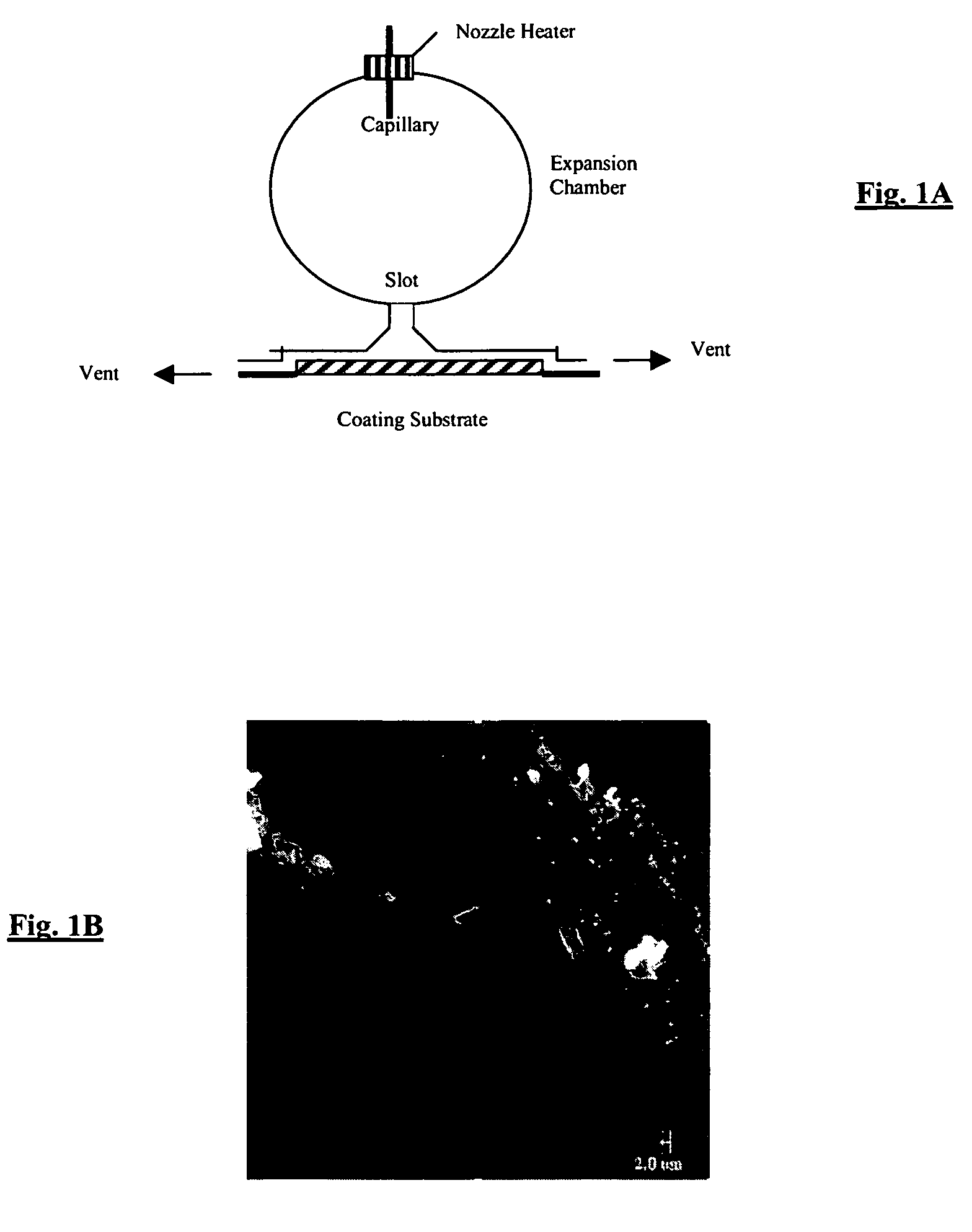
[0042]A nominally 1800 ml stainless steel particle formation vessel was fitted with a 4 cm diameter agitator of the type disclosed in U.S. Pat. No. 6,422,736, comprising a draft tube and bottom and top impellers. CO2 was added to the particle formation vessel while adjusting temperature to 90 C and pressure to 300 bar and while stirring at 2775 revolutions per minute. The addition of CO2 at 60 g / min through a feed port that had a 200 μm orifice at its tip, and a 0.1 wt % solution of Dye E and 0.01 wt % Cellulose Acetate Propionate binder (EASTMAN CAP 480-20) in acetone at 2 g / min, through a 100 μm tip, was then commenced, and the contents of the expansion chamber were exhausted from the chamber through an outlet port at an equivalent rate. The CO2 and solution feed ports were located close to the bottom impeller as disclosed for the inlet tubes for the mixer in U.S. Pat. No. 6,422,736, such that both the solution and the CO2 feed streams were introduced into a highly agitated zone w...
example 2
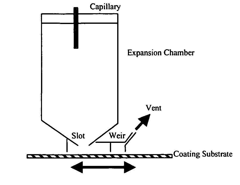
[0046]A nominally 1800 ml stainless steel particle formation vessel was fitted with a 4 cm diameter agitator of the type disclosed in U.S. Pat. No. 6,422,736, comprising a draft tube and bottom and top impellers. CO2 was added to the particle formation vessel while adjusting temperature to 90 C and pressure to 300 bar and while stirring at 2775 revolutions per minute. The addition of CO2 at 40 g / min through a feed port that had a 200 μm orifice at its tip, and a 0.1 wt % solution of Tert-Butyl-anthracene di-naphthylene (TBADN: a functional material used in Organic Light Emitting Diodes) in acetone at 2 g / min, through a 100 μm tip, was then commenced, and the contents of the expansion chamber were exhausted from the chamber through an outlet port at an equivalent rate. The CO2 and solution feed ports were located close to the bottom impeller as disclosed for the inlet tubes for the mixer in U.S. Pat. No. 6,422,736, such that both the solution and the CO2 feed streams were introduced ...
example 3
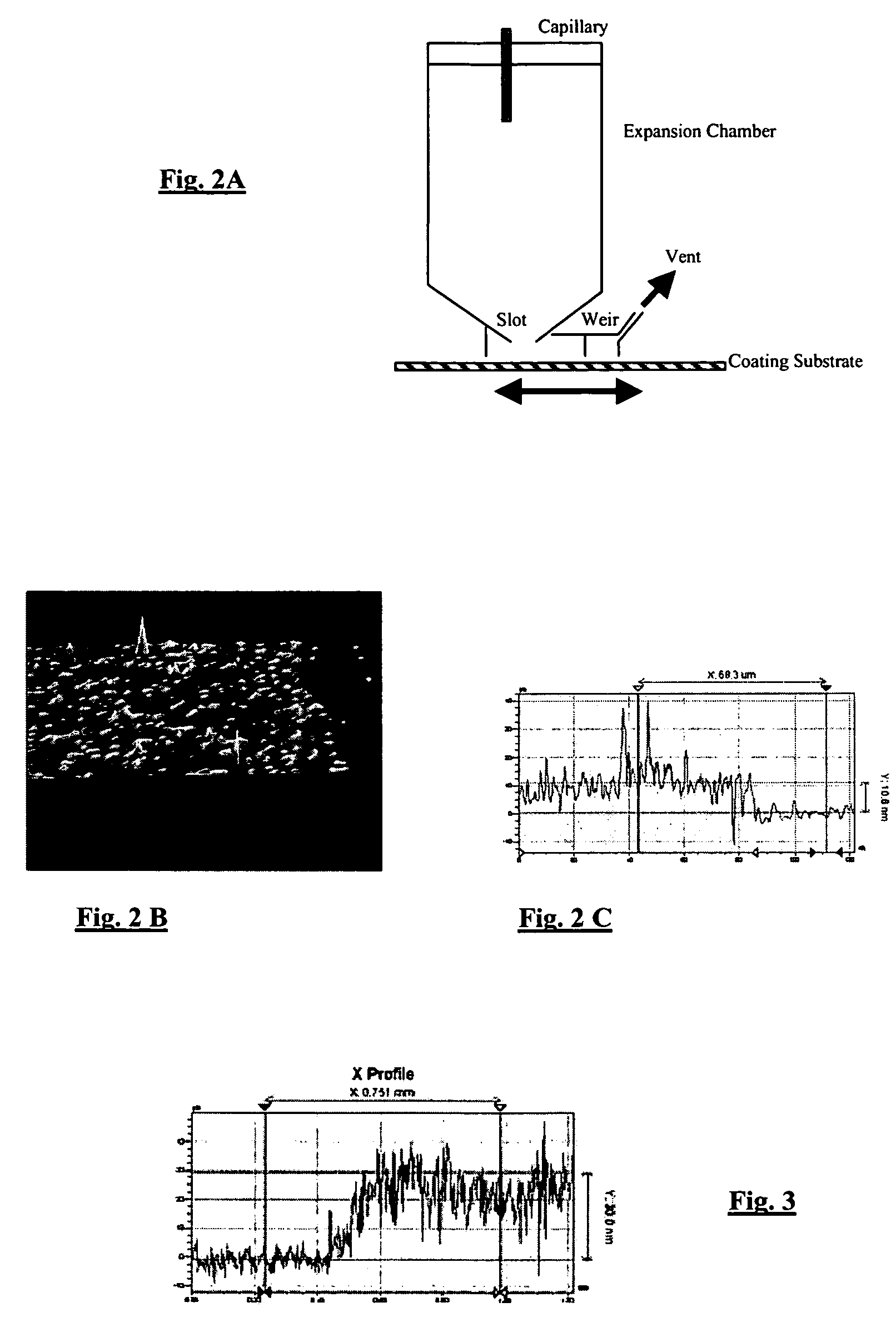
[0050]The procedure employed in Example 2 was repeated, except the functional material concentration was 0.05 wt % in acetone and the pre-expansion heater temperature was 180 C. The resulting coating on the glass slide was also similarly examined, but at a surface magnification of 100×. FIG. 3 shows the instrument signal near a carefully created edge on the deposition surface. The lower level of the signal corresponds to the bare surface. The higher level corresponds to the deposited layer. It shows a nominal layer thickness of 30 nm, and a layer that is also continuous. The average surface roughness of the 30 nm thick layer was 5.44 nm, calculated by WYCO NT1000 as the arithmetic average of the absolute values of the surface features from the mean plane.
PUM
| Property | Measurement | Unit |
|---|---|---|
| volume-weighted average diameter | aaaaa | aaaaa |
| volume-weighted average diameter | aaaaa | aaaaa |
| volume-weighted average diameter | aaaaa | aaaaa |
Abstract
Description
Claims
Application Information


