Eureka AIR delivers breakthrough ideas for toughest innovation challenges, trusted by R&D personnel around the world.

Optical semiconductor device

Inactive Publication Date: 2010-11-11
PANASONIC CORP
View PDF10 Cites 3 Cited by
  • Summary
  • Abstract
  • Description
  • Claims
  • Application Information

AI Technical Summary

Benefits of technology

[0022]As described above, light-receiving elements must have the capability of high light-receiving sensitivity, high speed response and low power consumption. As for high light-receiving sensitivity, short wavelength light such as blue light has larger energy per photon and holds a smaller number of photons for the same optical output power, compared to infrared and red light. Therefore, a smaller number of carriers are generated from photoelectric conversion, leading to reduced light-receiving sensitivity. Assuming that quantum efficiency is 100% (one electron-hole pair is generated from one photon), the light-receiving sensitivity to light having the aforementioned wavelengths is 0.63 A / W for infrared light, 0.52 A / W for red light and 0.33 A / W for blue light. For this reason, a structure ensuring high light-receiving sensitivity to short wavelength light is desired.

Problems solved by technology

Therefore, a smaller number of carriers are generated from photoelectric conversion, leading to reduced light-receiving sensitivity.
However, in the conventional optical semiconductor devices described above, the structure realizing high light-receiving sensitivity and high speed response to light of a wide range of wavelengths requires application of a high voltage to amplify photocurrent and increases power consumption as in Conventional Example 1.
However, in the optical semiconductor devices of the Conventional Examples, parasitic capacitance and parasitic resistance are not sufficiently reduced although consideration is made in regard to the cross-sectional structure.

Method used


Image

  • Optical semiconductor device
  • Optical semiconductor device
  • Optical semiconductor device

Examples


first embodiment

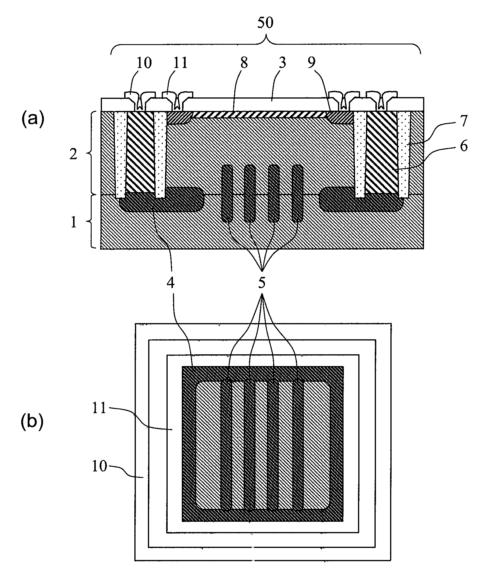
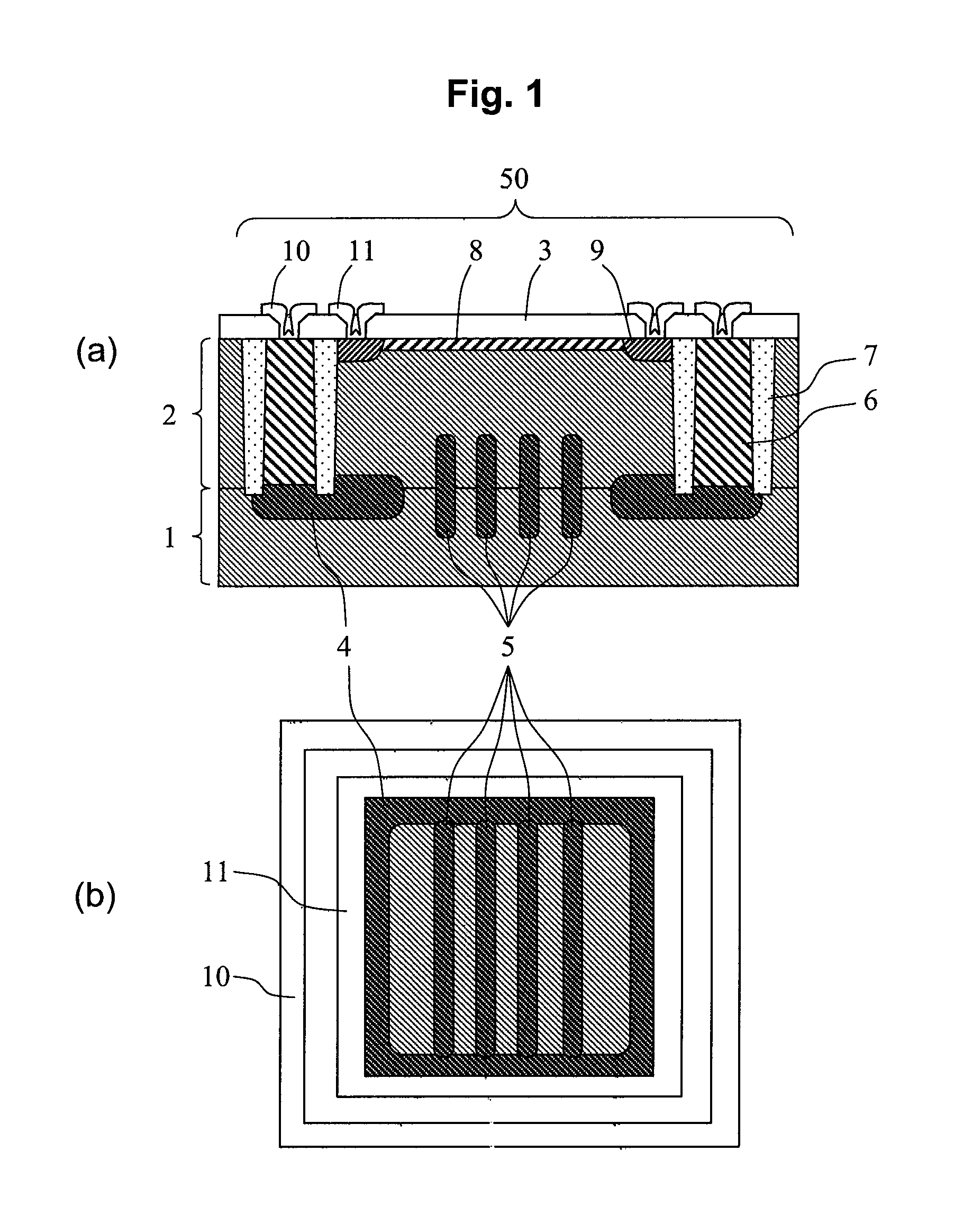
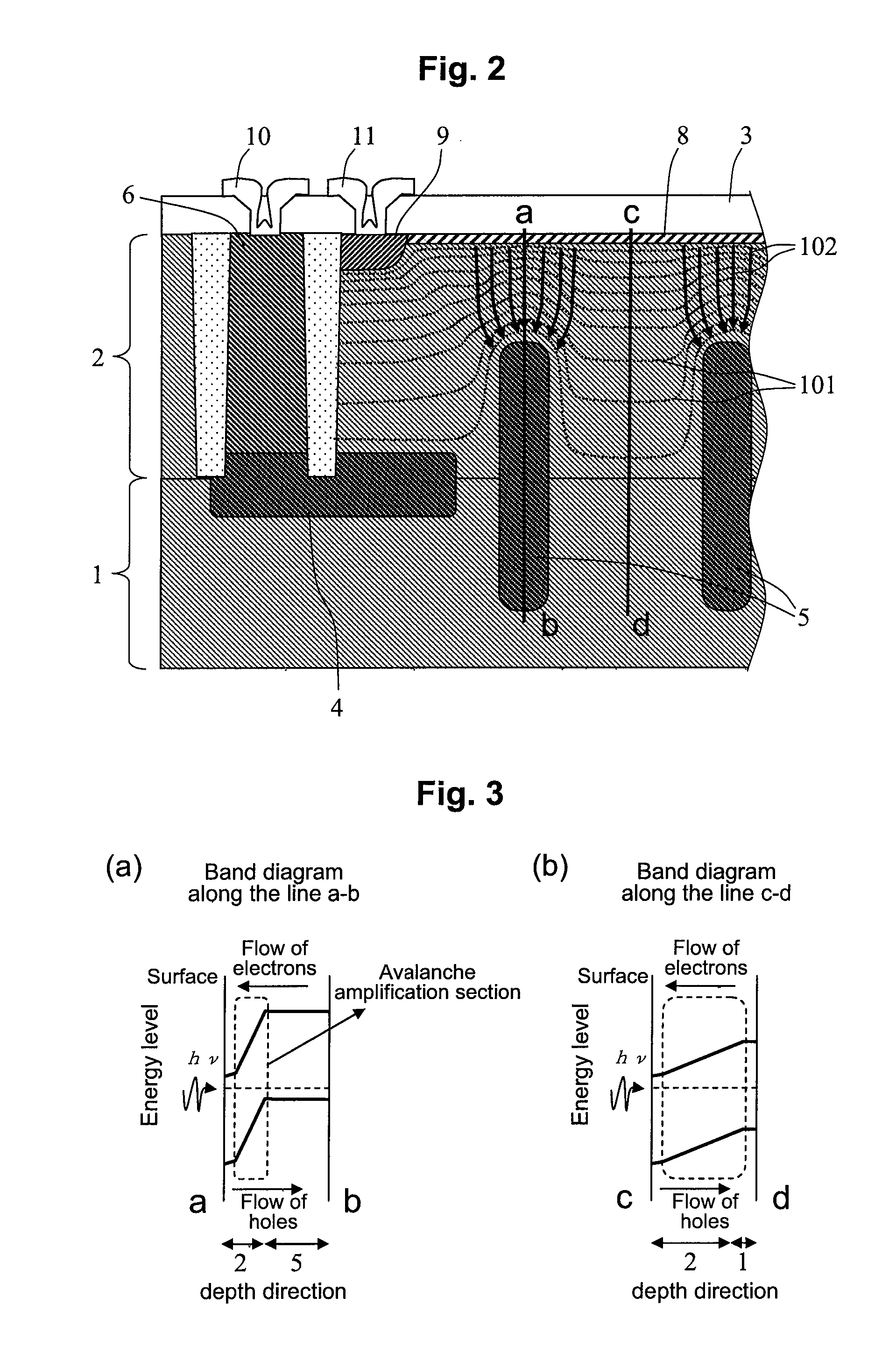
[0049]FIG. 1A is a cross-sectional view showing a light-receiving element of an optical semiconductor device in a first embodiment relating to the present invention. FIG. 1B is an illustration showing an exemplary planar layout of the light-receiving element. As described in detail hereafter, a light-receiving element portion 50 of this embodiment is characterized by a structure amplifying current using avalanche multiplication near a surface within a light-receiving region where incident light is converted to current signals.

[0050]As shown in the cross-sectional view of FIG. 1A, the device includes a P− type semiconductor substrate 1 consisting of a P type silicon (Si) having a low impurity concentration and a specific resistance of, for example, approximately 100 to 200 Ωcm, on which a P− type semiconductor layer 2 having a thickness of 2 μm and an impurity concentration equal to or lower than that of the P− type semiconductor substrate 1, for example, 1×1014 cm−3 is formed by usi...

second embodiment

[0071]FIG. 11 is a cross-sectional view of an optical semiconductor device (OEIC device) in the second embodiment relating to the present invention. The light-receiving element portion 50 of the optical semiconductor device according to the present invention is formed by selective ion implantation using a mask pattern through known production techniques as described above. Therefore, it can easily be integrated on the same substrate with bipolar transistors and MOS (metal oxide semiconductor) transistors, and these are formed in common process.

[0072]In FIG. 11, a first transistor portion 60 where an NPN bipolar transistor and a vertical PNP transistor are provided and a second transistor portion 70 where a CMOS transistor is provided are formed on a P− type semiconductor substrate 1 in addition to the light-receiving element portion 50. The light-receiving element portion 50, first transistor portion 60, and second transistor portion 70 are separated from each other by element separ...


PUM


Abstract

An optical semiconductor device comprises a first semiconductor region of a first conductivity type and a second semiconductor region of a second conductivity type formed on the first semiconductor region. The device further comprises a third semiconductor region of the first conductivity type formed in a semiconductor layer, which is separated from the first and second semiconductor regions by an element separation region, and a fourth semiconductor region of the first conductivity type formed between a semiconductor substrate and third semiconductor region. The device further comprises a fifth semiconductor region of the first conductivity type formed across the semiconductor substrate and the first semiconductor region. An upper portion of the fifth semiconductor region penetrates into a specific depth of the first semiconductor region. Amplification of a current signal occurs when a reverse voltage is applied between the second semiconductor region and a surface portion of the third semiconductor region.

Description

CROSS-REFERENCE TO RELATED APPLICATION[0001]This is a continuation of International Application No. PCT / JP2009 / 005313 filed on Oct. 13, 2009, which claims priority to Japanese Patent Application No. 2008-271798 filed on Oct. 22, 2008. The disclosures of these applications including specifications, drawings and claims are incorporated herein by reference in their entireties.BACKGROUND OF THE INVENTION[0002]1. Field of the Invention[0003]The present invention relates to an optical semiconductor device and particularly to an optical semiconductor device in which a light-receiving element and a logical element are formed on a same substrate.[0004]2. Description of the Related Art[0005]An opto-electronic integrated circuit (OEIC) device is a type of an optical semiconductor device, in which a light-receiving element such as a photodiode converting an optical signal to an electric signal, an active element such as a transistor element constituting a peripheral circuit, and a passive eleme...

Claims


Application Information

Patent Timeline
IPC IPC(8): H01L31/10H01L31/0352
CPCH01L31/107
Inventor MIYAJIMA, TSUTOMUYASUKAWA, HISATADA
Owner PANASONIC CORP
Why Eureka
Eureka Blog
Learn More