Thin film transistor, display, and electronic apparatus

a thin film transistor and electronic equipment technology, applied in the direction of transistors, electrical equipment, semiconductor devices, etc., can solve the problems of deterioration of transistor characteristics, amorphous oxide constituting the oxide semiconductor layer is susceptible to reduction, etc., and achieve the effect of maintaining long-term reliability and stable thin film transistor characteristics

Inactive Publication Date: 2010-11-25
JOLED INC
View PDF14 Cites 68 Cited by
  • Summary
  • Abstract
  • Description
  • Claims
  • Application Information

AI Technical Summary

Benefits of technology

[0009]In the thin film transistor according to the embodiment of the present invention as above-mentioned, iridium or iridium oxide constituting the source electrode and the drain electrode has a preventive effect on diffusion of reducing atoms or molecules, such as those of hydrogen and nitrogen, and on diffusion of oxygen. Therefore, reducing atoms or molecules such as those of hydrogen and nitrogen are prevented from being supplied through diffusion into the semiconductor layer having the amorphous oxide, and, simultaneously, oxygen is prevented from being lost through diffusion from the semiconductor layer having the amorphous oxide. As a result, the semiconductor layer having the amorphous oxide can be restrained from deterioration due to reduction and from deterioration due to oxygen defects.
[0010]Thus, according to embodiments of the present invention, the semiconductor layer having the amorphous oxide can be restrained from deterioration due to reduction and from deterioration due to oxygen defects, and, therefore, stability of thin film transistor characteristics can be maintained for a long period of time. In addition, it is made possible to maintain long-term reliability of the display and the electronic apparatus which are configured by use of the thin film transistor.

Problems solved by technology

However, the amorphous oxide constituting the oxide semiconductor layer is susceptible to reduction by hydrogen, nitrogen or the like.
Such reduction of the amorphous oxide would cause deterioration of the oxide semiconductor layer, which, in turn, leads to deterioration of transistor characteristics, such as scattering of threshold voltage of the thin film transistor or variations in current (Ids)-voltage (Vds) characteristic of the thin film transistor.

Method used


Image

  • Thin film transistor, display, and electronic apparatus
  • Thin film transistor, display, and electronic apparatus
  • Thin film transistor, display, and electronic apparatus

Examples


first embodiment

Modification of First Embodiment

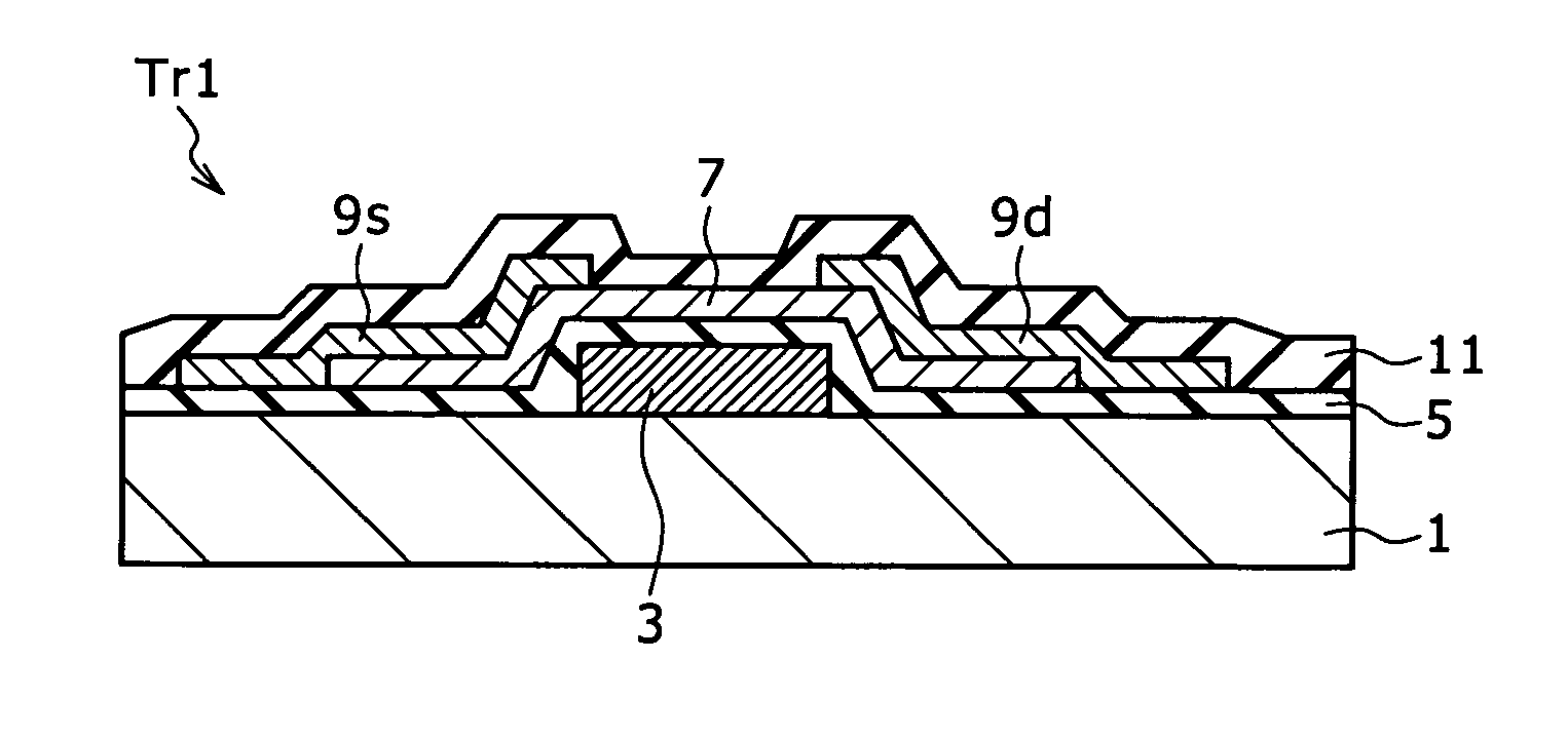
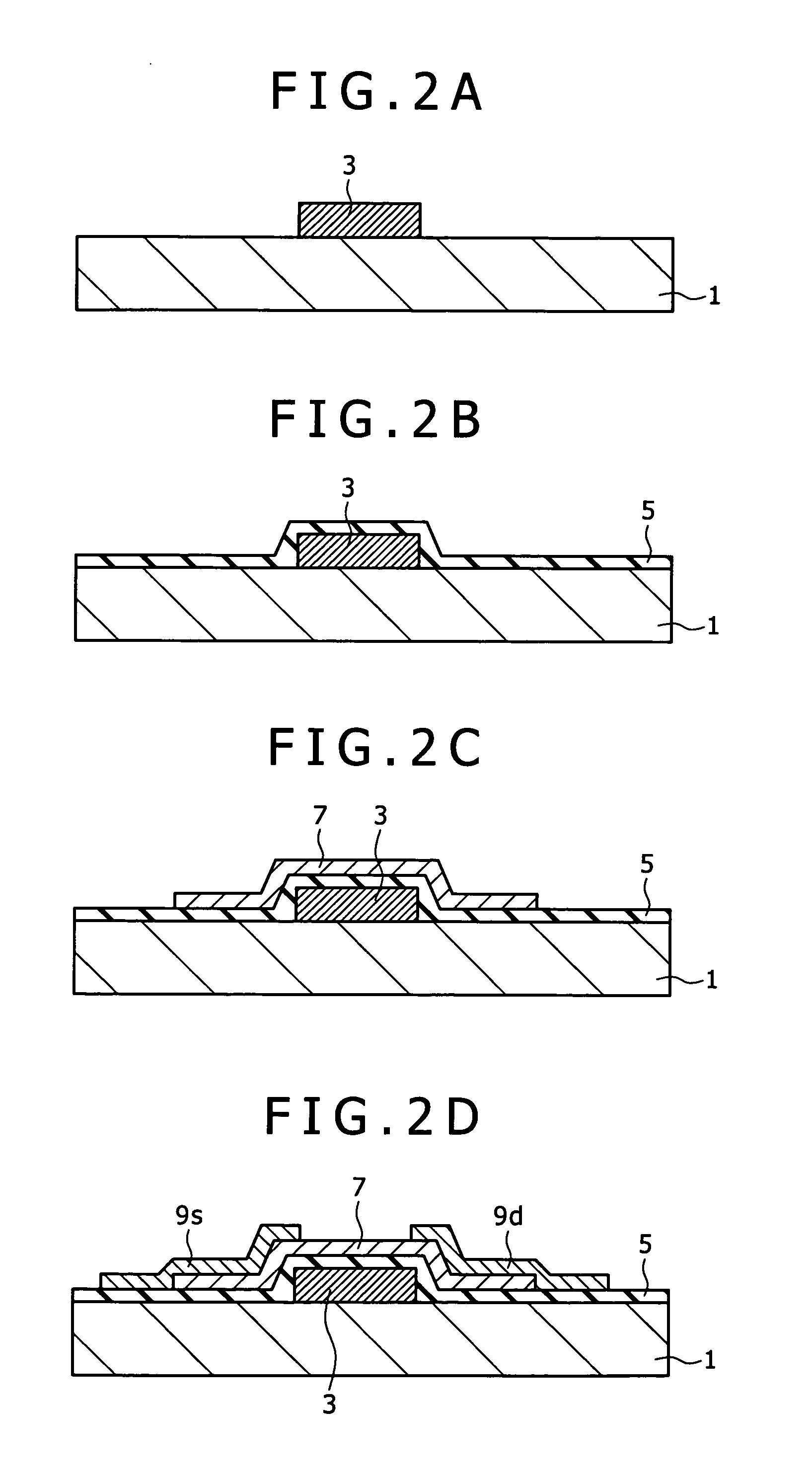
[0105]A thin film transistor Tr1′ shown in FIG. 3 is a modification of the bottom-gate thin film transistor described in the first embodiment above. The thin film transistor Tr1′ of the modification shown in FIG. 3 differs from the thin film transistor Tr1 shown of FIG. 1 in the order of stacking of the insulating film 11 covering the oxide semiconductor layer 7 and the source and drain electrodes 9s and 9d. Therefore, the components equivalent to those described above are denoted by the same reference symbols used above, and descriptions of them will be omitted.

[0106]A gate electrode 3 is formed in a pattern on a substrate 1, and a gate insulating film 5 having an oxide material is provided so as to cover the gate electrode 3. On the gate insulating film 5, a semiconductor layer 7 having an amorphous oxide (hereinafter referred to as oxide semiconductor layer) is provided on the upper side of the gate electrode 3. Besides, an insulating film 11 havin...

second embodiment

2. Second Embodiment

[0111]FIG. 4 is a sectional view of a thin film transistor Tr2 according to a second embodiment of the present invention. The thin film transistor Tr2 shown in the figure is a top-gate thin film transistor Tr2 in which a semiconductor layer having an amorphous oxide (oxide semiconductor layer) is used as an active layer, and which is configured as follows. Incidentally, the components the same as those in the first embodiment above are denoted by the same reference symbols as used above, and descriptions of these components will be omitted.

[0112]An insulating film 11 formed by use of an oxide material is provided on a substrate 1. Over the insulating film 11, a source electrode 9s and a drain electrode 9d are provided by use of iridium (Ir) or iridium oxide (IrO2), and, further, an oxide semiconductor layer 7 having an amorphous oxide is provided between and partly on the source electrode 9s and the drain electrode 9d. In addition, a gate insulating film 5 having...

third embodiment

3. Third Embodiment

[0132]FIG. 6 is a schematic sectional diagram, corresponding to two pixels, of a liquid crystal display 20-1 in which the bottom-gate thin film transistor Tr1 described in the first embodiment above is used. The liquid crystal display 20-1 according to this third embodiment of the present invention as shown in the figure has a configuration in which a substrate 1 provided thereon with the thin film transistors Tr1 of the first embodiment is used as a driving-side substrate, and a liquid crystal layer LC is sandwiched between the driving-side substrate 1 and an opposite substrate 30.

[0133]Of these components, the driving-side substrate 1 is configured as follows.

[0134]Each of pixels a on the driving-side substrate 1 has the thin film transistor Tr1 of the first embodiment and, also, a capacitance element Cs connected thereto. While the thin film transistor Tr1 of the first embodiment described above referring to FIG. 1 is shown here as an example of the thin film t...


PUM


Abstract

Disclosed herein is a thin film transistor including: a semiconductor layer including an amorphous oxide, and a source electrode and a drain electrode which are provided in contact with the semiconductor layer. The source electrode and the drain electrode are formed by use of iridium or iridium oxide.

Description

BACKGROUND OF THE INVENTION[0001]1. Field of the Invention[0002]The present invention relates to a thin film transistor using a semiconductor layer having an amorphous oxide, and to a display and an electronic apparatus which include the thin film transistor.[0003]2. Description of the Related Art[0004]Application of a semiconductor layer having an amorphous oxide (hereinafter referred to as oxide semiconductor layer) formed by using In, Zn, Ga and O as an active layer in thin film transistors for driving flat panel displays such as liquid crystal displays and organic EL (electroluminescence) displays, has been investigated. Since the oxide semiconductor layer is formed at room temperature by vapor deposition or sputtering, it can be formed on a plastic substrate. Besides, it is said that in this type of thin film transistor, Au / Ti, Pt / Ti, or zinc gallium oxide is used for forming source / drain electrodes provided in contact with the oxide semiconductor layer, and, therefore, good tr...

Claims


Application Information

Patent Timeline
Patent Type & Authority Applications(United States)
IPC IPC(8): H01L29/786H01L29/04H01L33/16H01L33/26
CPCH01L27/1225H01L27/124H01L29/78693H01L27/3244H10K59/12
Inventor HIRONAKA, KATSUYUKI
Owner JOLED INC
Why Eureka
Try Eureka