Photoelectric conversion device

a conversion device and photoelectric technology, applied in the direction of vehicle heating/cooling devices, transportation and packaging, road transportation emission reduction, etc., can solve the problems of poor conversion efficiency of photoelectric conversion devices using amorphous silicon, inconvenient installation in a limited area of vehicles, and single crystal solar cells with a thickness of hundreds of micrometers are not flexible, so as to achieve the effect of improving the thickness and flexibility of photoelectric conversion devices

Inactive Publication Date: 2010-12-09
SEMICON ENERGY LAB CO LTD
View PDF23 Cites 22 Cited by
  • Summary
  • Abstract
  • Description
  • Claims
  • Application Information

AI Technical Summary

Benefits of technology

[0009]It is an object of the present invention to provide a photoelectric conversion device which is thin, li

Problems solved by technology

However, while being lightweight and able to be installed on the curved surface, photoelectric conversion devices using amorphous silicon are poor in the conversion efficiency and are not suitable for installation in a limited area of vehicles or the l

Method used


Image

  • Photoelectric conversion device
  • Photoelectric conversion device
  • Photoelectric conversion device

Examples


Embodiment Construction

[0030]Hereinafter, embodiments of the present invention will be described with reference to accompanying drawings. Note that the present invention is not limited to the description below, and it is easily understood by those skilled in the art that a variety of changes and modifications can be made without departing from the spirit and scope of the present invention. Therefore, the present invention is not to be construed as being limited to the description of the embodiments below.

[0031]In the embodiments below, the same parts may be denoted by the same reference numerals throughout the drawings. Note that the thickness, the width, a relative position, and the like of components, that is, layers, regions, and the like illustrated in the drawings are exaggerated in some cases for clarification in the description of the embodiments.

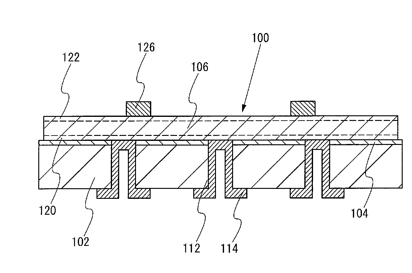
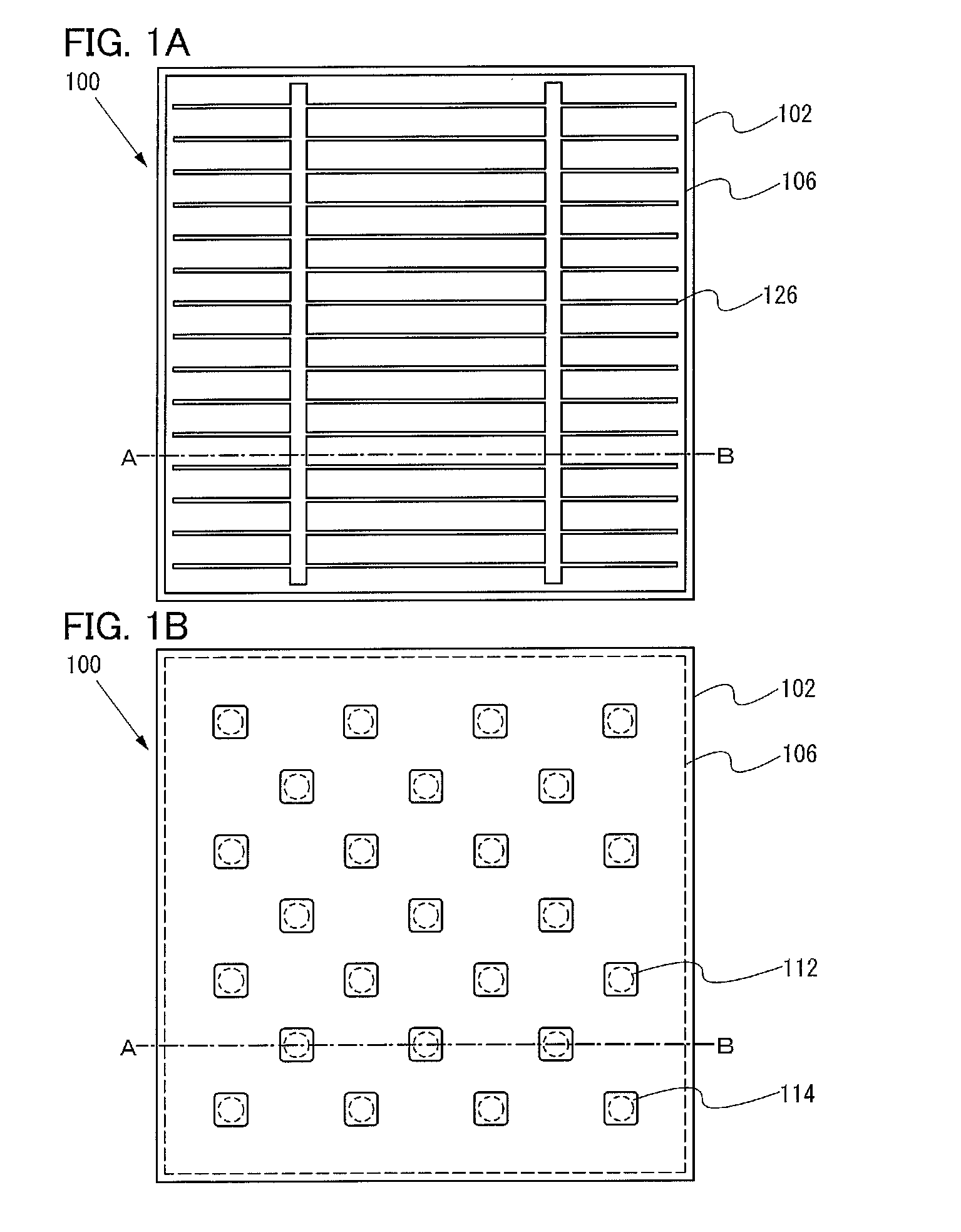
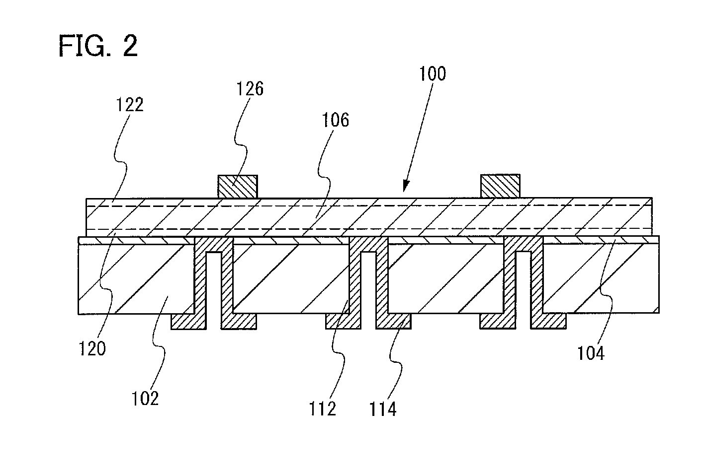
[0032]One mode of a photoelectric conversion device according to one embodiment will be described with reference to FIGS. 1A and 1B and FIG. 2. FIG. 1A is...


PUM


Abstract

A photoelectric conversion device which is thin, lightweight, and flexible even in the case of using a crystalline semiconductor such as single crystal silicon. A photoelectric conversion layer is provided in contact with an insulating film provided on one surface of a support substrate. An electrode (rear electrode) which is in contact with one surface of the photoelectric conversion layer is provided in accordance with a opening which passes through the support substrate and the insulating film. The rear electrode is in electrical contact with the photoelectric conversion layer and the support substrate. On the other surface of the photoelectric conversion layer, an electrode (surface electrode) on a light incidence side is provided. The photoelectric conversion layer is formed using a semiconductor material; preferably, a single crystal semiconductor or a polycrystalline semiconductor is used.

Description

BACKGROUND OF THE INVENTION[0001]1. Field of the Invention[0002]The present invention relates to a photoelectric conversion device using a photovoltaic effect of a semiconductor.[0003]2. Description of the Related Art[0004]Increasing consciousness of protection of the global environment through emission reduction of carbon dioxide draws attention to hybrid vehicles. Further, development of electric vehicles that are not powered by an internal-combustion engine has also been advanced. Regarding a photoelectric conversion device used as a power source for vehicles which are driven by electricity, not only high conversion efficiency of solar energy, but also lightness and installation so as to fit a curve of the vehicle body have been demanded.[0005]The following has been disclosed in Patent Document 1: a flexible solar cell in which amorphous silicon is formed on a plastic film substrate or a metal film substrate is used as a photoelectric conversion device for vehicles, for the above...

Claims


Application Information

Patent Timeline
IPC IPC(8): H01L31/00
CPCB60H1/00428H01L31/02008H01L31/022425Y02E10/50H01L31/042H01L31/0504H01L31/1896H01L31/03921Y02T10/88
Inventor ARAI, YASUYUKI
Owner SEMICON ENERGY LAB CO LTD
Why Eureka
Try Eureka