Hole Transport Polymer for Use in Electronic Devices

Inactive Publication Date: 2010-12-09
GOUGH NEIL
View PDF0 Cites 13 Cited by
  • Summary
  • Abstract
  • Description
  • Claims
  • Application Information

AI Technical Summary

Benefits of technology

[0018]As used herein, “layer” does not mean that a perfect layer of material is formed. Rather, as known in the art, certain defects such as pinholes or areas which do not have the material may be present, as long as the defects do not prevent the layer from having the desired characteristics. Also, “layer” may mean that in certain areas, there is more material thickness than in other areas. In specific embodiments, “layer” includes a partial layer up to multiple layers.
[0019]As used herein, when two moieties are “attached,” it is to be understood that there is not necessarily a covalent bond between the two moieties. The term “attach” and its grammatical variations refers to a coupling or joining of two or more chemical or physical elements. In some instances, attach can refer to a coupling of two or more atoms based on an attractive interaction, such that these atoms can form a stable structure. Examples of attachment includes chemical bonds such as chemisorptive bonds, covalent bonds, ionic bonds, van der Waals bonds, and hydrogen bonds. Additional examples of attachment include various mechanical, physical, and electrical couplings. Spin-coating, or vapor depositing one substance onto another is an example of “attached.”
[0020]The overall fabrication and arrangement of an OLED is known in the art using materials and techniques known in the art. Some examples are given here, however, all suitable known embodiments and components are intended to be included here. The substrate may be rigid or flexible. As is known in the art, a device may contain more than one layer that may be characterized as having the same technical function. For example, there may be more than one different layers in a device that function as an “emissive layer.” All such embodiments are intended to be included here. The structures corresponding to abbreviations used are known in the art. All useful combinations of the various components and layers are intended to be included to the extent as if they were specifically listed.

Problems solved by technology

Vapor deposition provides for a well-defined layer structure possessing excellent purity; however this methodology is only applicable to low molecular mass molecules possessing high thermal stability [13].

Method used


Image

  • Hole Transport Polymer for Use in Electronic Devices
  • Hole Transport Polymer for Use in Electronic Devices
  • Hole Transport Polymer for Use in Electronic Devices

Examples


examples

[0045]The following examples are provided to illustrate some non-limiting embodiments of the invention. In the Schemes, exemplary reactions and reagents are shown. Methods of synthesis of various compounds is known in the art.

Synthesis of 9-(4-nitrophenyl)-9H-carbazole (2)

[0046]Sodium hydride (1.85 g, 0.077 mol) was added to a solution of carbazole (11.70 g, 0.070 mol) in N,N-dimethylformamide (DMF) (100.0 ml) and the reaction mixture stirred at room temperature under an atmosphere of dry nitrogen for ten minutes. 1-Fluoro-4-nitrobenzene (7.53 ml, 0.071 mol) was added in portions and the reaction mixture heated under reflux for 16 h, cooled to room temperature and poured onto water (300 ml). The precipitate was collected by filtration and re-crystallized repeatedly from acetonitrile. 1H NMR (500 MHz, CDCl3) δ / ppm: 8.49-8.51 (dt, 2H, aromatic), 8.15-8.17 (dt, 2H, aromatic), 7.81-7.83 (dt, 2H, aromatic), 7.45-7.52 (m, 4H, aromatic), 7.35-7.38 (td, 2H, aromatic).

Synthesis of 4-(9H-carb...


PUM

PropertyMeasurementUnit
Roughnessaaaaaaaaaa
pressureaaaaaaaaaa
electroluminescentaaaaaaaaaa

Abstract

Organic light emitting diode (OLED) devices are one of the most promising alternatives to liquid crystal displays (LCDs) for flat panel display (FPD) applications. The OLED technique is based on organic semiconductors used either as hole- or electron transporting materials or as an emitter. Working on common problems of performance and life time in OLED preparation, improved charge transport molecules and polymers such as triarylamine- and poly(para-phenylene)-have been developed. Some useful materials include: (1) cyclic triarylamine-derivatives possessing enhanced glass transition temperatures; (2) triarylamine based low molecular mass hole-transport molecules and hole-transport polymers with pendant oxetane groups for processing out of solution and subsequent cross-linking; and (3) fluorenyl-segmented poly(para-phenylene)s with defined electrochemical properties. Provided is a polymer precursor that is useful as a hole transport polymer in OLED and other organic electronic devices.

Description

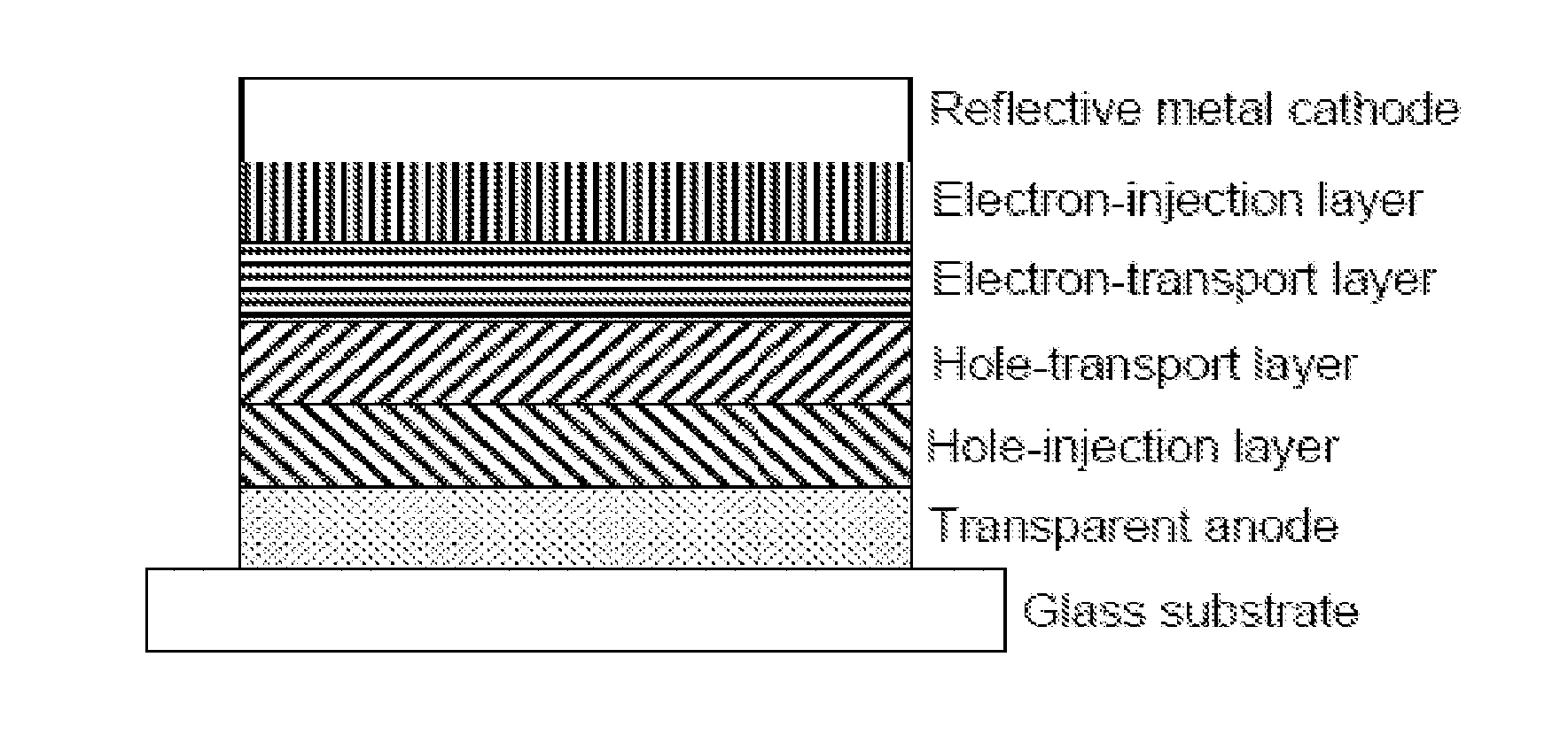
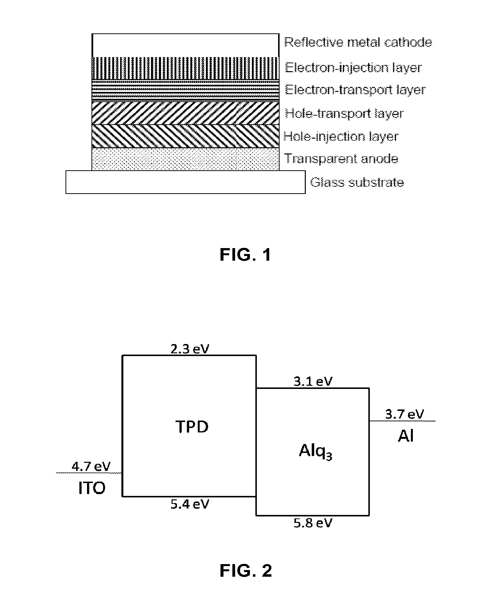
BACKGROUND OF THE INVENTION[0001]Organic light-emitting diodes (OLEDs) are currently being widely investigated for many applications such as in the flat-panel display industry, particularly for applications which require low power consumption, high color purity and long lifetime. The basic structure of a multilayer OLED was introduced by Eastman-Kodak in 1987[3] and is based on electroluminescent and semi-conducting organic materials packed between two electrodes as shown in FIG. 1. After charge injection from the electrodes into the organic layer and charge migration within the respective layers (FIG. 2) electrons and deficient electrons (‘holes’) can combine to form an excited singlet state. Light emission of the latter is then as a result of relaxation processes [1, 2].[0002]In order to achieve high electroluminescence efficiency and long life time, the materials have to fulfill several specific requirements [4], which include low injection barriers at the interfaces between elec...

Claims


Application Information

Patent Timeline
Patent Type & Authority Applications(United States)
IPC IPC(8): H05B37/00H01B1/12H01L51/40H01L51/54
CPCC07D209/82H01L51/004Y02E10/549H01L51/0072H01L51/0081H01L51/0059H10K85/141H10K85/631H10K85/6572H10K85/324
Inventor GOUGH, NEILTSAI, ETHANHUFFMAN, WILLIAM A.WILLIAMS, CHRISTOPHER D.DAMERON, ARRELAINE A.
Owner GOUGH NEIL
Why Eureka
Try Eureka