Surface Plasmon Enhanced Optical Devices for Integrated Photonics
a surface plasmon and photonics technology, applied in the field of optical devices, can solve the problems of increased device density, large loss, destructive interference and therefore isolation, etc., and achieve the effect of reducing the size and cost of the optical system, and increasing the complexity of the optical system
- Summary
- Abstract
- Description
- Claims
- Application Information
AI Technical Summary
Benefits of technology
Problems solved by technology
Method used
Image
Examples
Embodiment Construction
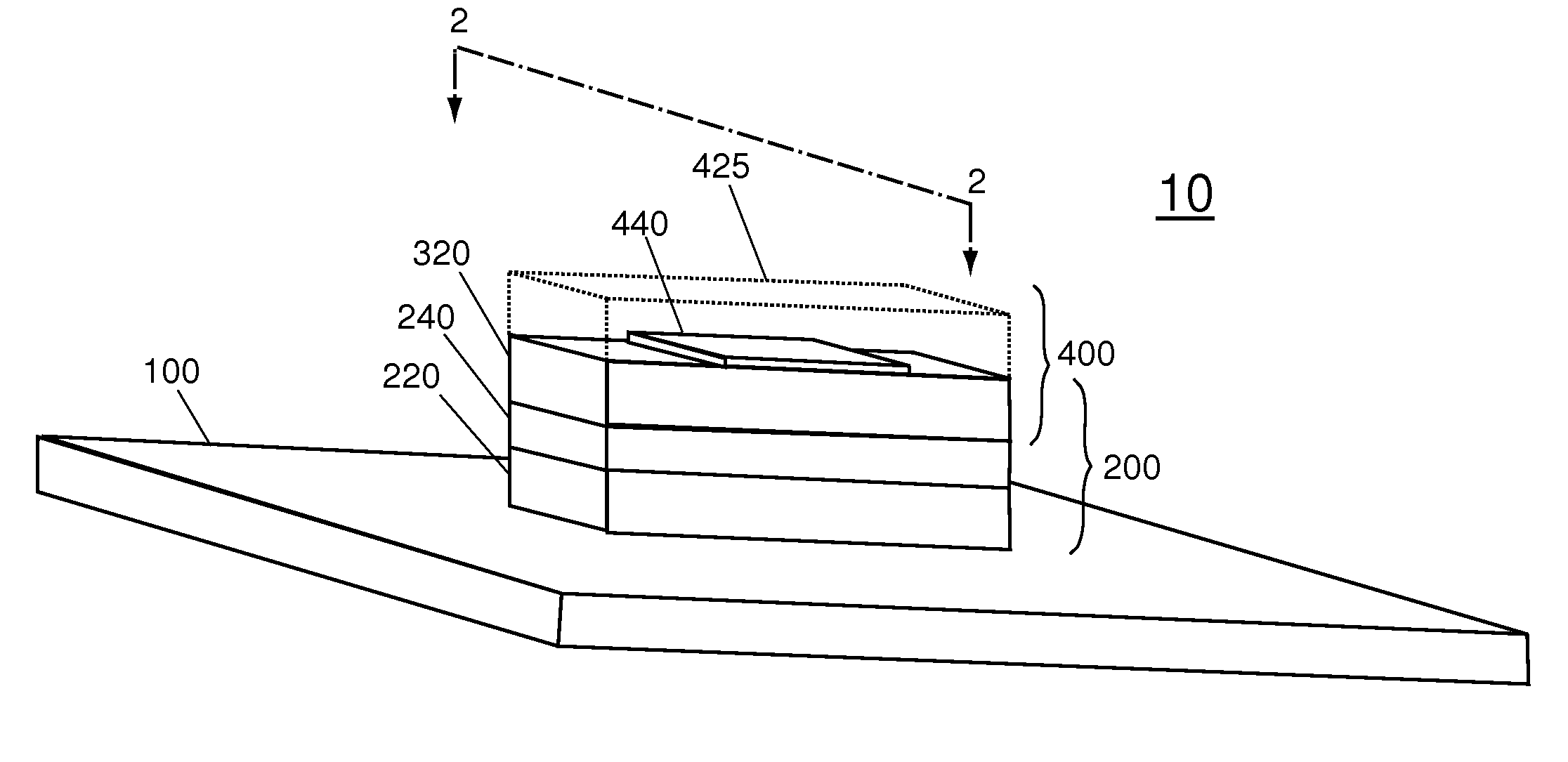
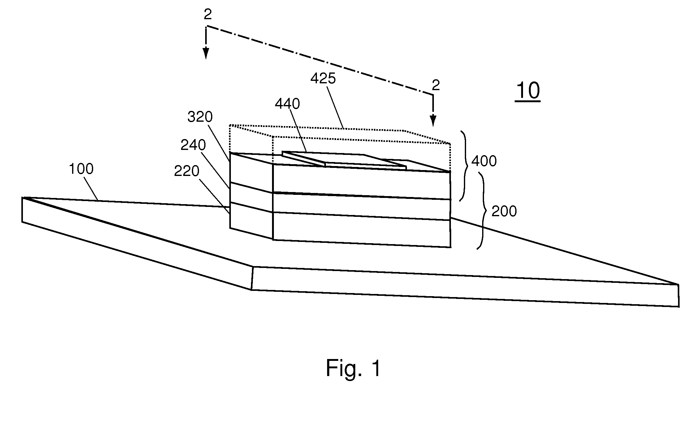
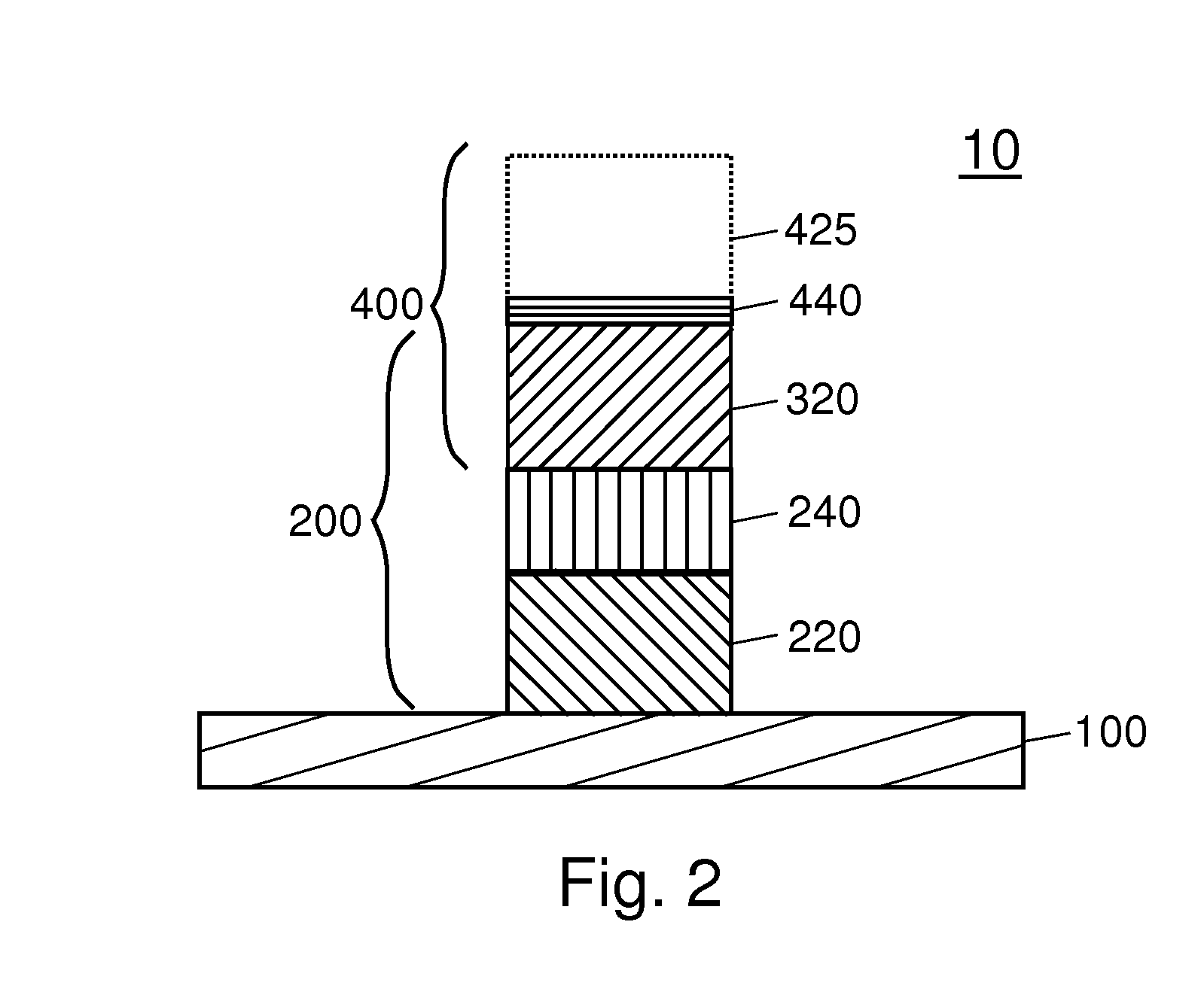
[0069]FIG. 1 shows an optical device 10, e.g., an isolator, fabricated on substrate 100 and exploits a nonreciprocal coupling from a dielectric waveguide 200 into a surface plasmon waveguide 400 to achieve large isolation in the reverse direction and low insertion loss in the forward direction. FIG. 2 depicts the optical device 10 in cross sectional view with the ridge width. The two waveguides are designed to share a common cladding 320. The dielectric waveguide 200 includes three dielectric layers referred to as dielectric waveguide cladding 220, dielectric waveguide core 240, and the common cladding 320. The surface plasmon waveguide 400 includes three layers referred to as effective surface plasmon cladding 425, surface plasmon core 440, and the common cladding 320.
[0070]The optical device 10 is compatible with fabrication techniques developed for the semiconductor industry on substrate 100. In various embodiments, substrate 100 can be InP, GaAs, Si, GaSb, GaN, or other like mat...
PUM
| Property | Measurement | Unit |
|---|---|---|
| insertion loss | aaaaa | aaaaa |
| insertion loss | aaaaa | aaaaa |
| thickness | aaaaa | aaaaa |
Abstract
Description
Claims
Application Information


