
Eureka
For R&D, Eureka makes reading and utilizing patents & technical documents easy.
Eureka AIR
Designed for self-driven R&D workflows. Generate viable solutions, solve complex R&D challenges, empower your innovation with AI.

Eureka Materials
Designed for material experts only. Revolutionize your material R&D, from search, analyze, to developing new materials.

TechResearch
Generate reliable direction feasibility study reports for your R&D in just a few steps.

TechSeek
Discover and master advanced knowledge NOW. Basics, ideas, possibilities, all at once.

TechMind
As an expert in R&D Theories, TechMind can generates customized viable solutions instantly.

TechRisk
Analyze your overall solution with one click, know your potential R&D risks in advance.

TechMonitor
Get weekly tech updates, stay abreast of the latest tech innovations and key insights.
Copper alloy material for electric/electronic components
- Summary
- Abstract
- Description
- Claims
- Application Information
AI Technical Summary
Benefits of technology
Problems solved by technology
Method used
Image

Examples
example 1
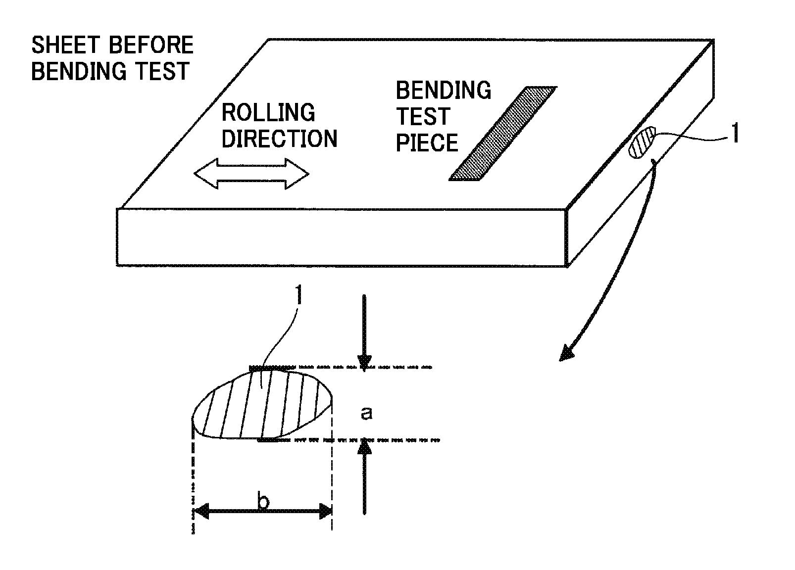
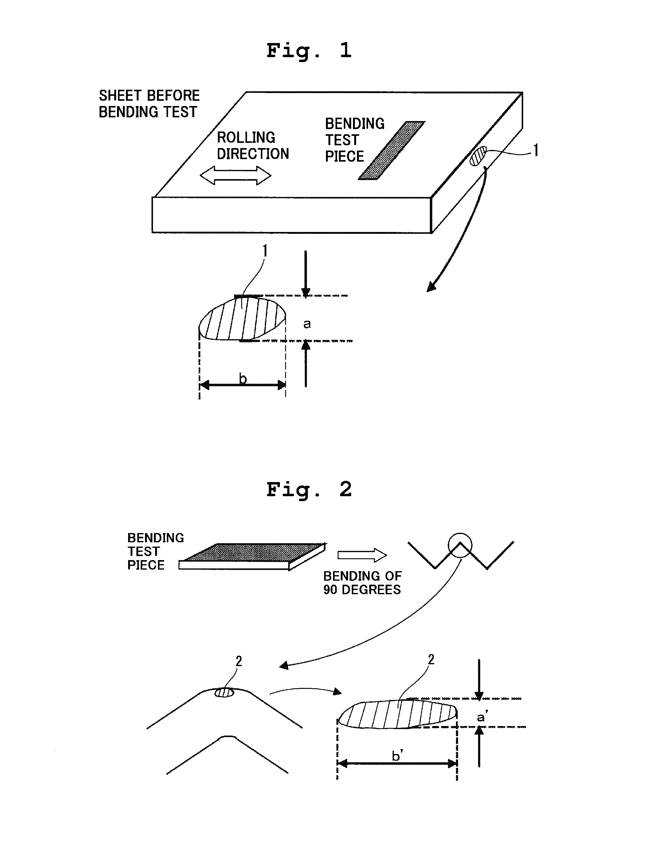
[0084]Here, each of the copper alloys which is made use for the corresponding Examples (the present invention examples and the comparative examples) in accordance with the present invention is formed of an alloy (the present invention examples No. 1 to 30 and the comparative examples No. 1 to 30) which contains a component that is shown in the following Table 1 and the Table 2 respectively, and contains a remaining portion which is formed of Cu and an unavoidable impurity, respectively. Moreover, each of those alloys is dissolved by making use of a high frequency melting furnace, and then thereafter each of these is casted with a cooling rate between 10° C. per second and 30° C. per second to obtain an ingot which has a dimension of a thickness of 30 mm and a width of 120 mm and a length of 150 mm, respectively.
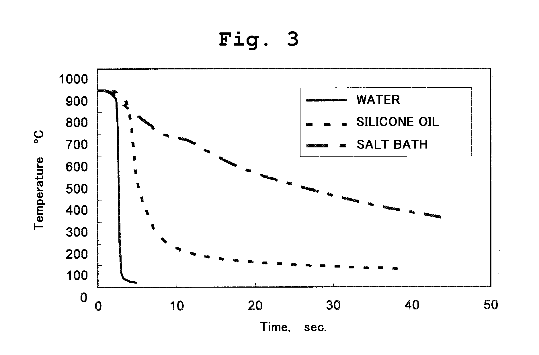
[0085]Next, each of those obtained ingots is maintained at a temperature between 930° C. and 970° C. with an amount of time between 0.5 hour and 1 hour, and then the hot roll...
PUM
| Property | Measurement | Unit |
|---|---|---|
| Temperature | aaaaa | aaaaa |
| Temperature | aaaaa | aaaaa |
| Length | aaaaa | aaaaa |
Abstract
Description
Claims
Application Information
 - R&D Engineer
- R&D Manager
- IP Professional
- Industry Leading Data Capabilities
- Powerful AI technology
- Patent DNA Extraction
Browse by: Latest US Patents, China's latest patents, Technical Efficacy Thesaurus, Application Domain, Technology Topic, Popular Technical Reports.
© 2024 PatSnap. All rights reserved.Legal|Privacy policy|Modern Slavery Act Transparency Statement|Sitemap|About US| Contact US: help@patsnap.com