System for directly measuring the depth of a high aspect ratio etched feature on a wafer

a technology of etched feature and wafer, which is applied in the direction of optical radiation measurement, semiconductor/solid-state device testing/measurement, instruments, etc., can solve the problems of large or small reflected light amplitude, and achieve the effect of simple, accurate and reliabl

Inactive Publication Date: 2010-12-23
RUDOLPH TECHNOLOGIES INC
View PDF4 Cites 22 Cited by
  • Summary
  • Abstract
  • Description
  • Claims
  • Application Information

AI Technical Summary

Benefits of technology

[0025]To produce a sufficient interference signal, which is observed through the fringe visibility of the reflected signal, the reflections from the wafer's upper and lower surfaces must have similar beam divergences. For example, if the incident beam is collimated, then the reflected beams from the two surfaces will be collimated, and the interference will be strong and fringe visibility high. However, the present invention requires the incident beam to be focused so that only a small area is illuminated and the etched feature can be spatially distinguished. For substrates that are thicker than the depth of focus, the two reflections have different divergence angles, and so the fringe visibility is reduced. The depth of focus of a focused beam in a medium is approximately proportional to:DOF=λn2NA2,
[0026]where λ is the wavelength, n is the index of refraction of the medium, and NA is the numerical aperture of the focusing lens. Thus, the depth of focus increases with the index of refraction of the medium, which is approximately 3.6 for silicon. For example, if the numerical aperture is 0.1, and the wavelength 1.31 μm, then the depth of focus in silicon is approximately 468 μm. As a result, a silicon wafer can be as thick as 1000 μm and the fringe visibility would still be strong enough to provide a good signal.
[0029]By placing the sensor so that it faces the non-etched surface, the etched feature appears to be a bump in the etched surface of the wafer from the point of view of the sensor. Thus, there is no sidewall interference that inhibits optical techniques now employed and the bottom of the etched feature is easily illuminated regardless of the etched feature's depth.
[0035]is relatively easy to learn and operate when compared to similar systems,
[0038]is accurate, repeatable, non-destructive and has a high spatial resolution, and

Problems solved by technology

These reflections interfere with each other, and the reflected light amplitude can be large or small depending on whether the interference is constructive or destructive.

Method used


Image

  • System for directly measuring the depth of a high aspect ratio etched feature on a wafer
  • System for directly measuring the depth of a high aspect ratio etched feature on a wafer
  • System for directly measuring the depth of a high aspect ratio etched feature on a wafer

Examples


second embodiment

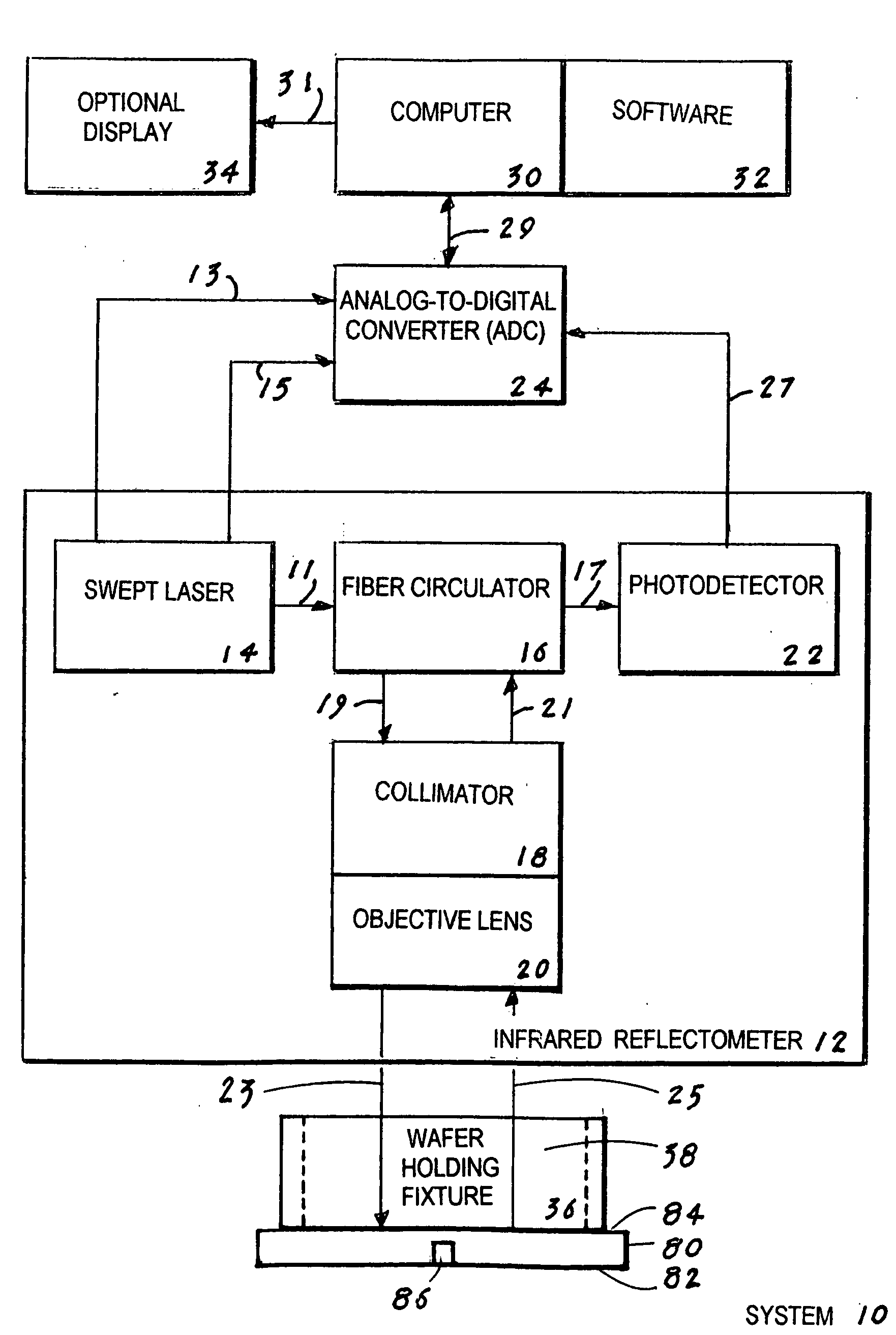
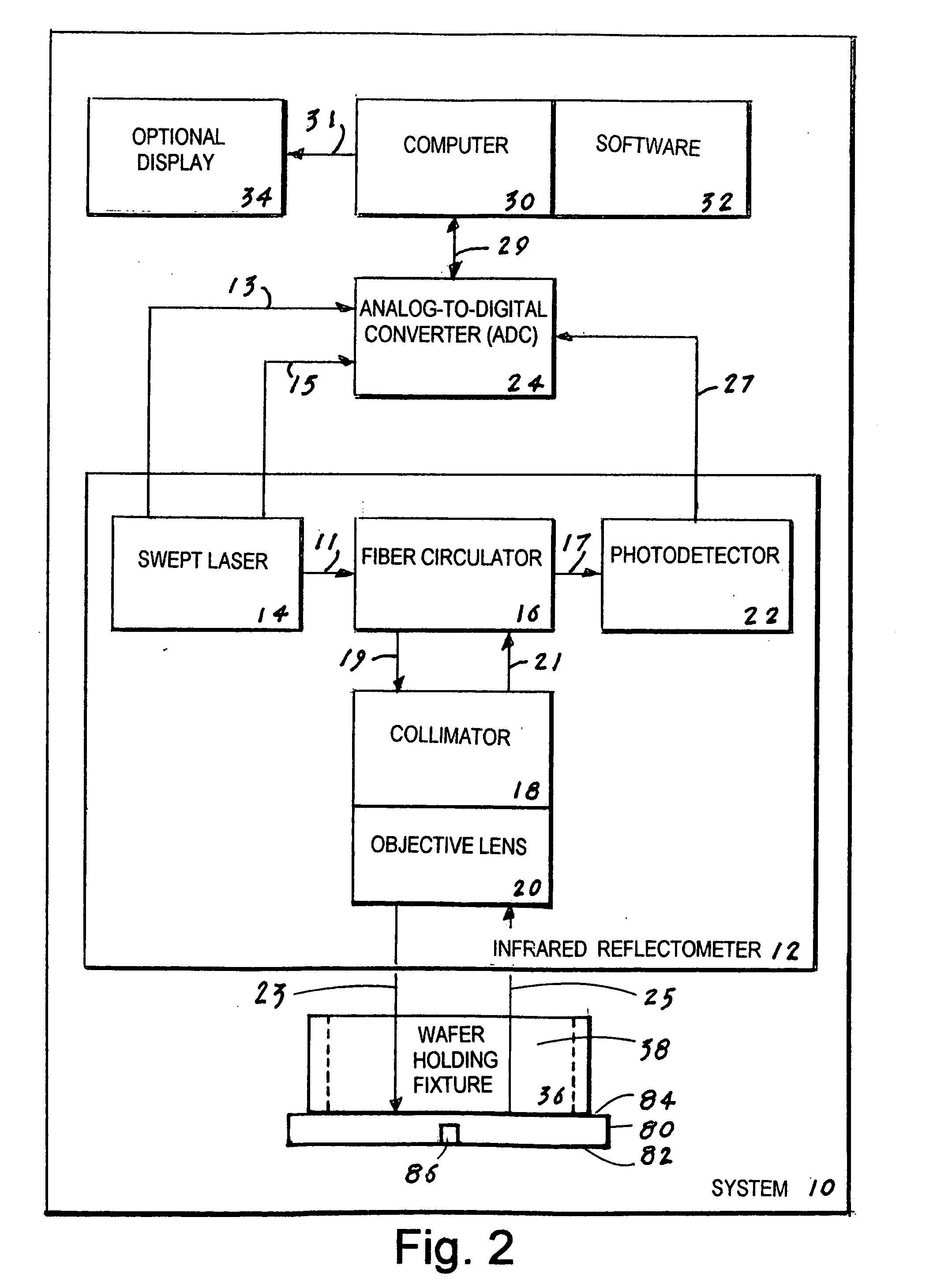
[0059]The second embodiment which is the preferred embodiment of the system 10, as shown in FIG. 2, is comprised of the following elements: an infrared reflectometer 12, a swept laser 14, a fiber circulator 16, a collimator 18, an objective lens 20, a photodetector 22, an ADC 24, a computer 30, software 32, a display 34 and a wafer holding fixture 36.

[0060]The infrared reflectometer 12 is designed to produce a focused incident light 23 and to receive a reflected light 25 and indicate their ratio. The reflectometer 12 uses a small spot size to illuminate the non-etched surface 84 of the wafer 80. The reflectometer 12 in the second embodiment is comprised of the swept laser 14 which produces a set of wavelengths 11 that are swept in time, a trigger signal 13 and a clock signal 15. The swept wavelengths 11 typically range from 1260 mm to 1360 mm which encompasses a range where the wafer 80 is transparent.

[0061]The fiber circulator 16 has a first input that receives the range of wavelen...

third embodiment

[0065]The third embodiment, as shown in FIG. 3, is comprised of the following elements: a broadband incoherent infrared source (BIIS) 40, a fiber circulator 16, a collimator 18, an objective lens 20, a spectrometer 42, a computer 30, software 32, a display 34 and a wafer holding fixture 36.

[0066]The broadband incoherent infrared source (BIIS) 40 has means for producing an incoherent light 35 that is applied to the first input of the fiber circulator 16. The fiber circulator has a first light output 19 which is directed the light to the collimator 18. The collimator 18 collimates the light which is then focused by the objective lens 20 to produce a focused incident light 23 that is applied to the non-etched surface 84 of the wafer 80. From the wafer 80 is produced a reflected light 25 that is composed of reflections from the non-etched surface 84, the etched surface 82, and any other layers that might comprise the wafer 80. The reflected light 25 is collected by the objective lens 20...


PUM


Abstract

A system (10) for directly measuring the depth of a high aspect ratio etched feature on a wafer (80) that includes an etched surface (82) and a non-etched surface (84). The system (10) utilizes an infrared reflectometer (12) that in a preferred embodiment includes a swept laser (14), a fiber circulator (16), a photodetector (22) and a combination collimator (18) and an objective lens (20). From the objective lens (20) a focused incident light (23) is produced that is applied to the non-etched surface (84) of the wafer (80). From the wafer (80) is produced a reflected light (25) that is processed through the reflectometer (12) and applied to an ADC (24) where a corresponding digital data signal (29) is produced. The digital data signal (29) is applied to a computer (30) that, in combination with software (32), measures the depth of the etched feature that is then viewed on a display (34).

Description

TECHNICAL FIELD[0001]The invention generally pertains to systems for measuring an etched feature on a wafer, and more particularly to a system that directly measures the depth of a high aspect ratio etched feature from the non-etched surface of a wafer.BACKGROUND ART[0002]In the field of electronics, one of the most sought after goals is miniaturization. Efforts to make electronics and electronic memory smaller continue to drive manufacturers. There are a variety of techniques and technologies that faciltate continued miniaturization. One technique that is growing in importance is the deep etching of wafers, and the volume of wafers that go through this process is increasing. As the lateral dimensions of the etched features on a wafer, including etched features, continue to decrease, the ability to control the etching process is becoming more difficult.[0003]For companies that make wafers with narrow deep etches, if the aspect ratio, which is defined as the ratio of etched depth to ...

Claims


Application Information

Patent Timeline
Patent Type & Authority Applications(United States)
IPC IPC(8): G01B11/22G01B11/00G01B11/02G01J3/00G06F15/00
CPCG01B2210/56G01B11/22H01L22/12H01L22/26
Inventor MARX, DAVID S.GRANT, DAVID L.
Owner RUDOLPH TECHNOLOGIES INC
Why Eureka
Try Eureka