Semiconductor storage device

a semiconductor storage device and storage device technology, applied in the field of semiconductor storage devices, can solve the problems of inability to maintain low latency, and achieve the effect of high-speed operation and low latency of semiconductor storage devices

Inactive Publication Date: 2010-12-23
RENESAS ELECTRONICS CORP
View PDF5 Cites 34 Cited by
  • Summary
  • Abstract
  • Description
  • Claims
  • Application Information

AI Technical Summary

Benefits of technology

[0008]In a general configuration of an SRAM (Static Random Access Memory) as an example of a semiconductor storage device, a common terminal is used as a data input terminal and a data output terminal. In an SRAM of the QDR (Quad Data Rate) system, a data input terminal and a data output terminal are separated and operated at double data rates, thereby realizing high-speed operation. In the DDR operation, data is transmitted / received at each of the rising and trailing edges of a clock signal. The inventors of the present invention have examined higher-speed operation and lower latency in the QDR system.
[0011]An object of the present invention is to provide a technique for realizing high-speed operation and low latency of a semiconductor storage device employing the QDR method.
[0014]A semiconductor storage device according to the present invention includes a memory cell array, a first buffer, a second buffer, a first circuit, a second circuit, a first DLL circuit, and a second DLL circuit. The first DLL circuit generates a first internal clock signal so as to reduce a phase difference between a first clock signal fetched via the first buffer and the first internal clock signal transmitted to the first circuit. The second DLL circuit generates the second internal clock signal so as to reduce a phase difference between the second clock signal fetched via the second buffer and the second internal clock signal transmitted to the second circuit. By adjusting the timing of the first internal clock signal, the input setup and hold time can be shortened. In a state where low latency is maintained, the frequency of a clock signal can be further increased. As a result, realization of high-speed operation and low latency of the semiconductor storage device employing the QDR method is achieved.
[0016]The present invention can provide a technique realizing high-speed operation and low latency of a semiconductor storage device employing the QDR method.

Problems solved by technology

Consequently, when the frequency of a clock signal supplied to an SRAM is increased for higher speed of the SRAM, low latency cannot be maintained.

Method used


Image

  • Semiconductor storage device
  • Semiconductor storage device
  • Semiconductor storage device

Examples


first embodiment

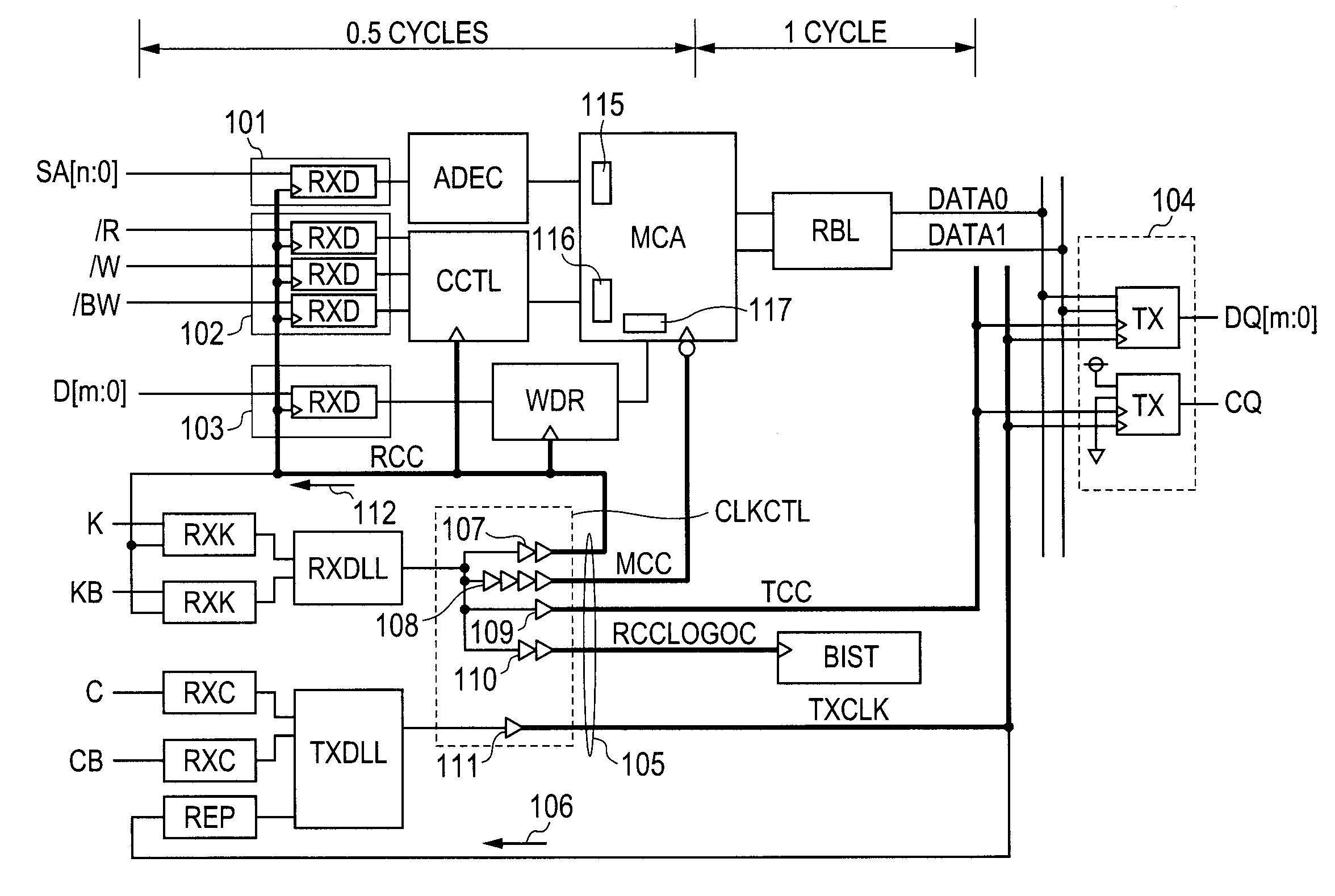
[0043]FIG. 1 shows an SRAM as an example of the semiconductor storage device according to the invention.

[0044]The SRAM shown in FIG. 1 is, although not limited, formed on a semiconductor substrate as one of single crystal silicon substrates by the known semiconductor integrated circuit manufacturing technique.

[0045]An address input buffer 101 is provided, which includes an input circuit RXD for fetching an address signal input via an external terminal synchronously with an internal clock signal RCC. A command input buffer 102 is provided, which includes a plurality of input circuits RXD for fetching various command signals input via external terminals synchronously with the internal clock signal RCC. The various command signals include a read signal / R instructing reading (“ / ” indicates an active low signal), a write signal / W instructing writing, and a bite write signal / BW instructing byte writing. A data input buffer 103 is provided and includes an input circuit RXD for fetching ...

second embodiment

[0082]FIG. 5 illustrates another configuration example of an SRAM as an example of a semiconductor storage device according to the present invention.

[0083]The configuration shown in FIG. 5 is largely different from that of FIG. 1 with respect to the point that latency can be switched. The clock control circuit CLKCTL changes latency by changing delay time in a delay circuit on the inside in accordance with a latency selection signal SEL.

[0084]FIG. 12 shows a configuration example of the clock control circuit CLKCTL in FIG. 5.

[0085]As shown in FIG. 12, the clock control circuit CLKCTL includes a plurality of delay circuits 131 to 140 and selectors 121 to 125. The delay circuit 131 is configured by two buffers, and the delay circuit 132 is configured by four buffers. The delay circuit 133 is configured by five buffers, and the delay circuit 134 is configured by one inverter. The delay circuit 135 is configured by one buffer, and the delay circuit 136 is configured by three buffers and...

third embodiment

[0087]FIG. 6 illustrates another configuration example of an SRAM as an example of a semiconductor storage device according to the present invention.

[0088]The SRAM shown in FIG. 6 is largely different from that of FIG. 1 with respect to the point that the internal clock signal MCC is generated by using an output signal of the output DLL circuit TXDLL. The internal clock signal MCC is delayed by a delay circuit 601 and transmitted via the clock tree 105 to the command control circuit CCTL, the write data register WDR, and the memory cell array MCA. The delay circuit 601 is formed by one inverter. The internal clock control circuit RCCLOGIC is delayed by a delay circuit 602 and transmitted via the clock tree 105 to the self diagnosis circuit BIST. The delay circuit 602 is formed by two buffers. The internal clock signal TXCLK is delayed by a delay circuit 603 and transmitted to the data output buffer 104 via the clock tree 105. The delay circuit 603 is formed by three buffers.

[0089]Wi...


PUM


Abstract

The present invention is directed to realize high-speed operation and low latency of a semiconductor storage device employing the QDR method. A memory cell array, a first buffer, a second buffer, a first circuit, a second circuit, a first DLL circuit, and a second DLL circuit are provided. The first DLL circuit generates a first internal clock signal so as to reduce a phase difference between a first clock signal fetched via the first buffer and the first internal clock signal transmitted to the first circuit. The second DLL circuit generates the second internal clock signal so as to reduce a phase difference between the second clock signal fetched via the second buffer and the second internal clock signal transmitted to the second circuit. With the configuration, input setup and hold time can be shortened, and the frequency of the clock signal can be further increased.

Description

CROSS-REFERENCE TO RELATED APPLICATIONS[0001]The disclosure of Japanese Patent Application No. 2009-146809 filed on Jun. 19, 2009 including the specification, drawings and abstract is incorporated herein by reference in its entirety.BACKGROUND OF THE INVENTION[0002]The present invention relates to a semiconductor storage device and, more particularly, to a technique for realizing high-speed operation and low latency in the semiconductor storage device.[0003]A semiconductor storage device can perform high-speed operation since it electrically records data by using semiconductor elements. In such a semiconductor storage device, there is a case where a DLL (Delay Locked Loop) circuit for adjusting timing of a clock signal is provided.[0004]Patent document 1 describes a technique of providing a delay fixed loop assuring operation margin which allows generation of a rising / polling out enable signal by a clock signal whose timing is adjusted by a DLL circuit even when the frequency of an ...

Claims


Application Information

Patent Timeline
Patent Type & Authority Applications(United States)
IPC IPC(8): G11C8/18G11C7/00
CPCG11C7/22G11C2207/2272G11C7/222
Inventor SHINOZAKI, MASAOSATO, HAJIME
Owner RENESAS ELECTRONICS CORP
Why Eureka
Try Eureka