Sealed plasma coatings

a technology of sealed plasma and coatings, applied in the direction of superimposed coating process, plasma technique, coatings, etc., can solve the problems of affecting the yield of the coating, and affecting the quality of the coating

Inactive Publication Date: 2010-12-23
SAINT GOBAIN CERAMICS & PLASTICS INC
View PDF12 Cites 42 Cited by
  • Summary
  • Abstract
  • Description
  • Claims
  • Application Information

AI Technical Summary

Benefits of technology

[0015]In another aspect, a method of forming an electronic device can include providing an electrostatic chuck defining a work surface, providing a workpiece overlying the work surface, providing a voltage across the electrostatic chuck and the workpiece to maintain the workpiece in proximity to the work surface; and processing the workpiece to form an electronic device. The electrostatic chuck can include (i) an insulating layer having an aspect ratio of at least 1.1, (ii) a conductive layer overlying the insulating layer, (iii) a dielectric layer have pores forming interconnected porosity overlying the conductive layer, and (iv) a sealant residing in the pores of the dielectric layer. In a particular embodiment, the sealant can be a thermally cured sealant having a cure temperature not greater than about 120° C. In another particular embodiment, the sealant can be an epoxy sealant having a viscosity of not greater than 500 cP in liquid precursor form. In yet another particular embodiment, the sealant can be a low shrinkage sealant characterized by a solidification shrinkage of not greater than 8%.

Problems solved by technology

In some process chamber environments, for example, halogen containing high-density plasma-etching chamber environments, conditions are highly aggressive, causing erosion of various chamber components, including chamber walls, liners, process kits, dielectric windows, and chucks.
Mechanical chucks have a disadvantage in that they often cause distortion of workpieces due to non-uniform forces being applied to the wafers.
Thus, wafers are often chipped or otherwise damaged, resulting in a lower yield.
In this respect, pressures in the chamber during semiconductor manufacturing processes tend to be low, and sufficient force cannot always be applied.
This shift to processing of larger workpieces, generally within high temperature and corrosive processing environments, places further demands on chamber components used during processing.

Method used


Image

  • Sealed plasma coatings
  • Sealed plasma coatings
  • Sealed plasma coatings

Examples


examples

[0069]The following examples based are based on coupons samples to illustrate concepts of present invention. It is understood that commercial samples would be in the form of completed electrostatic chucks having the requisite features for usage.

[0070]Example 1, comparative samples, no infiltration.

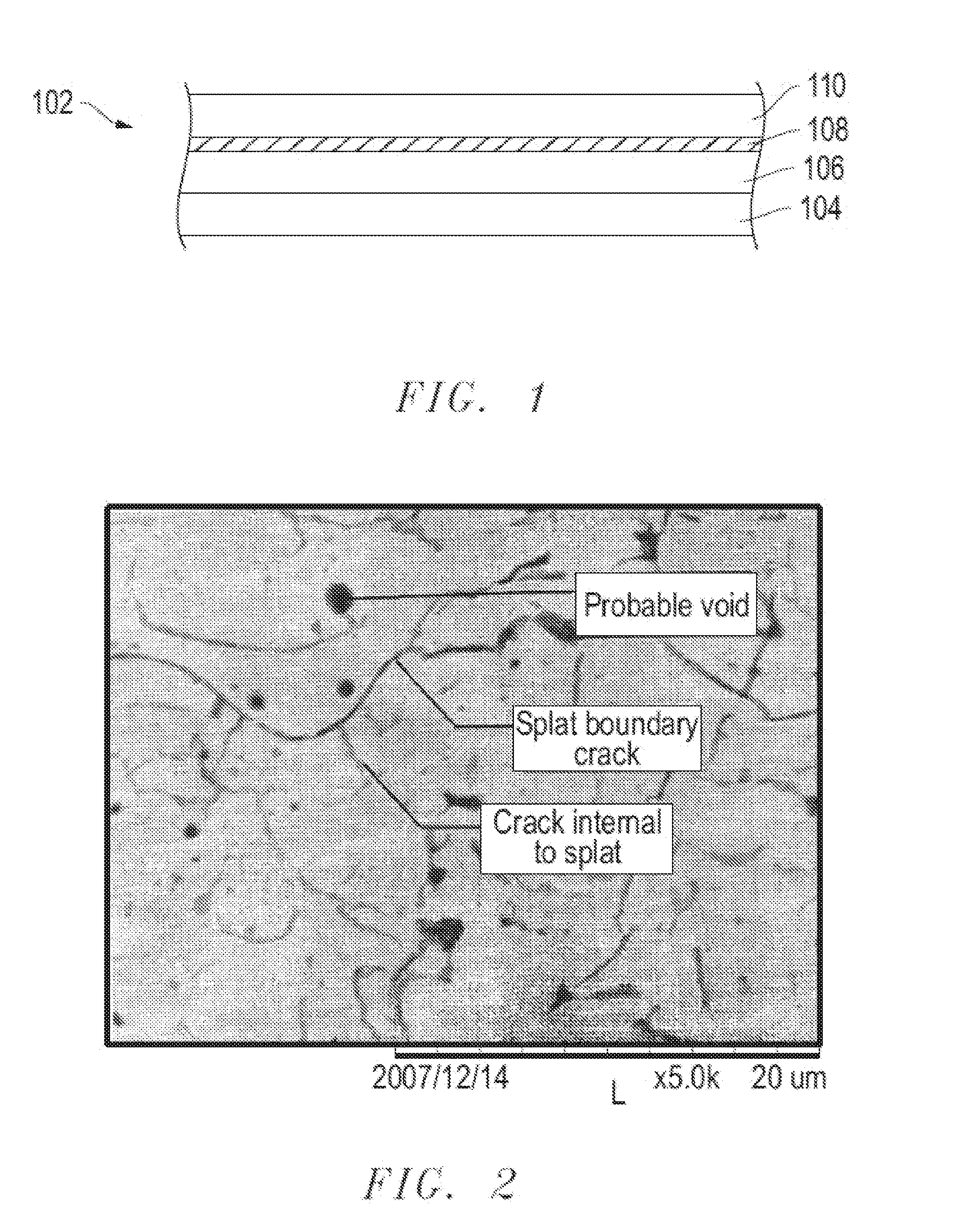
[0071]Four 6061 aluminum squares 4 cm on a side were grit blasted, plasma sprayed with aluminum oxide to a thickness of about 500 um to provide a porosity about 5%, and then plasma sprayed with tungsten on top to a thickness of about 50 um.

[0072]The samples were tested by applying a steadily increasing DC voltage between the tungsten and the base aluminum and monitoring current. Breakdown was deemed to occur when the current exceeded 2 mA.

TABLE 1Comparative SampleBreakdown voltage (kV)H2.5K10.3N4.7O2.1

[0073]The breakdown voltage varies, with a mean value of only 4.9 kV

[0074]Example 2, samples with infiltration.

[0075]Three samples were prepared as for example 1, but with the following addit...


PUM

PropertyMeasurementUnit
temperatureaaaaaaaaaa
pore sizeaaaaaaaaaa
thicknessaaaaaaaaaa

Abstract

A processing device includes a plurality of walls defining an interior space configured to be exposed to plasma and a surface coating on the interior surface of at least one of the plurality of walls. The surface coating includes pores forming interconnected porosity. The processing device further includes a sealant residing in at least a portion of the pores of the surface coating. In an embodiment, the sealant can be a thermally cured sealant having a cure temperature not greater than about 100° C. In another embodiment, the sealant can be an epoxy sealant having a viscosity of not greater than 500 cP in liquid precursor form. In yet another embodiment, the sealant can be a low shrinkage sealant characterized by a solidification shrinkage of not greater than 8%.

Description

CROSS-REFERENCE TO RELATED APPLICATION(S)[0001]The present application claims priority from U.S. Provisional Patent Application No. 61 / 218,598, filed Jun. 19, 2009, entitled “Sealed plasma coatings,” naming inventors Ara Vartabedian, Marc Abouaf, Stephen W. Into and Matthew A. Simpson, which application is incorporated by reference herein in its entirety.BACKGROUND[0002]1. Field of the Disclosure[0003]This disclosure is directed to sealed plasma coatings and is particularly directed to sealed plasma coatings for electrostatic chucks and plasma chamber walls for use in processing of flat panel display glass and semiconductor wafers.[0004]2. Description of the Related Art[0005]During semiconductor processing, various steps involve the use of plasmas, such as plasma etch, plasma-enhanced chemical vapor deposition (PECVD) and resist strip. The equipment required for these processes must operate within an environment inside the plasma chamber. Inside the plasma chamber, the equipment can...

Claims


Application Information

Patent Timeline
Patent Type & Authority Applications(United States)
IPC IPC(8): C23C16/458H01L21/683C23C16/00
CPCC23C4/18H01J37/321H01J37/32495H01L21/6833C23C28/3455C23C28/321C23C28/322C23C28/345C23C28/042
Inventor VARTABEDIAN, ARAABOUAF, MARCINTO, STEPHEN W.SIMPSON, MATTHEW A.
Owner SAINT GOBAIN CERAMICS & PLASTICS INC
Why Eureka
Try Eureka