

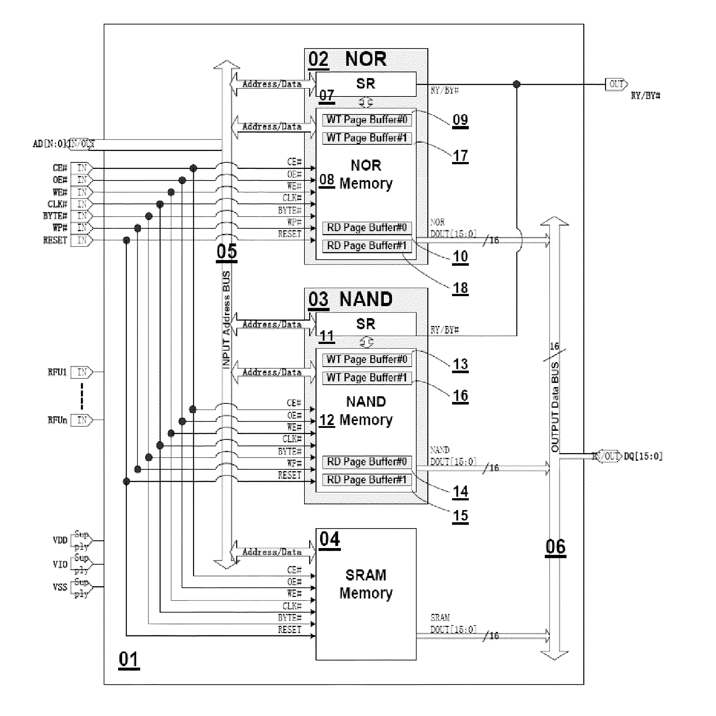
Memory system having NAND-based nor and NAND flashes and SRAM integrated in one chip for hybrid data, code and cache storage
a memory system and nand flash technology, applied in the memory field, can solve the problems of not being compatible with nand, nor and sram, unable to be integrated into one chip, and becoming more and more difficult to scale down below 45 nm technology, etc., to achieve more independent and faster operations, improve system response speed, and improve memory read and write operation speed.
- Summary
- Abstract
- Description
- Claims
- Application Information
AI Technical Summary
Benefits of technology
Problems solved by technology
Method used
Image

Examples
Embodiment Construction
[0067]Hereinafter, exemplary embodiments of the present invention will be described in detail. However, the present invention is not limited to the embodiments disclosed below, and can be implemented in various forms. The following embodiments are described in order to enable those of ordinary skill in the art to embody and practice the present invention.
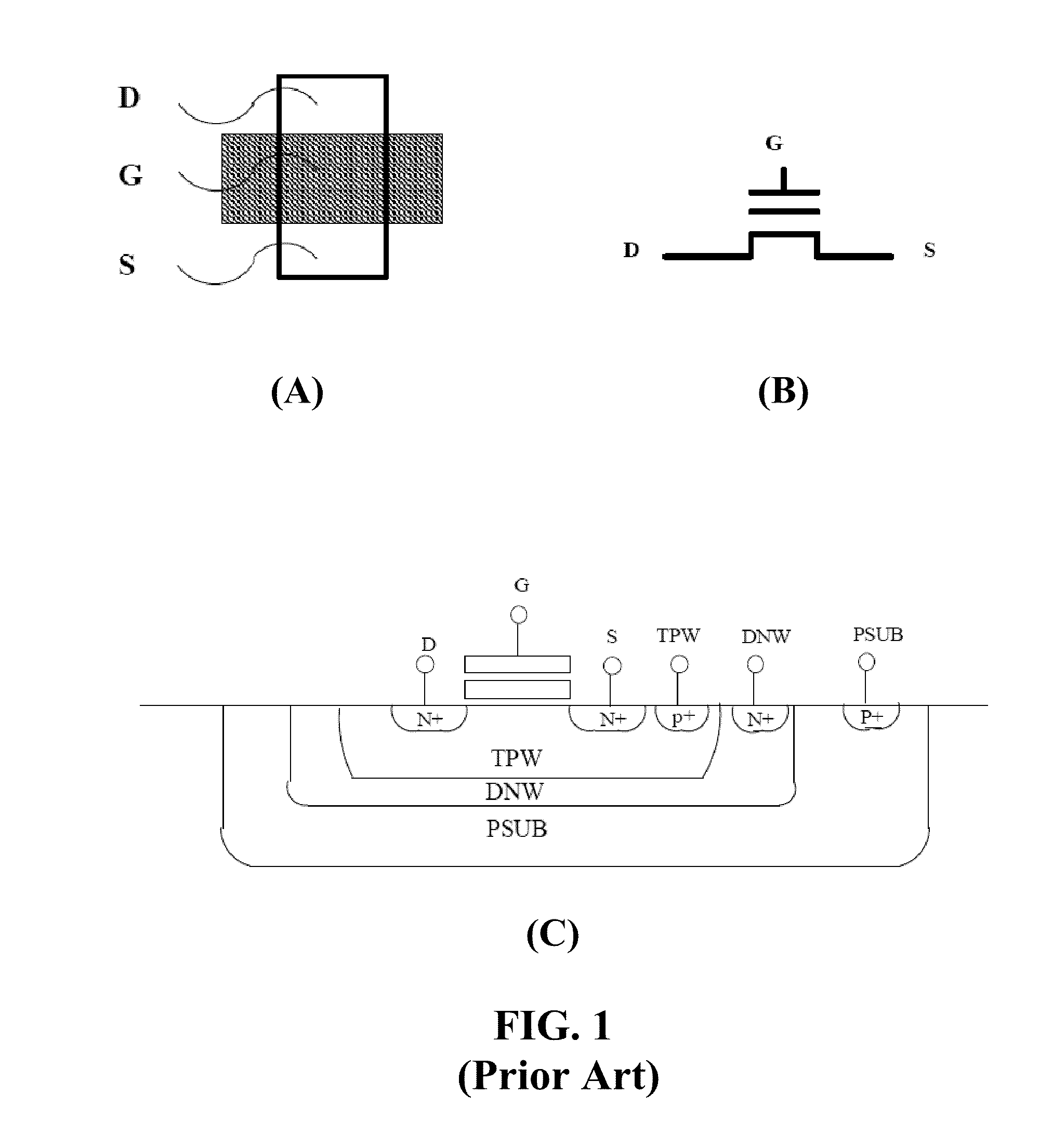
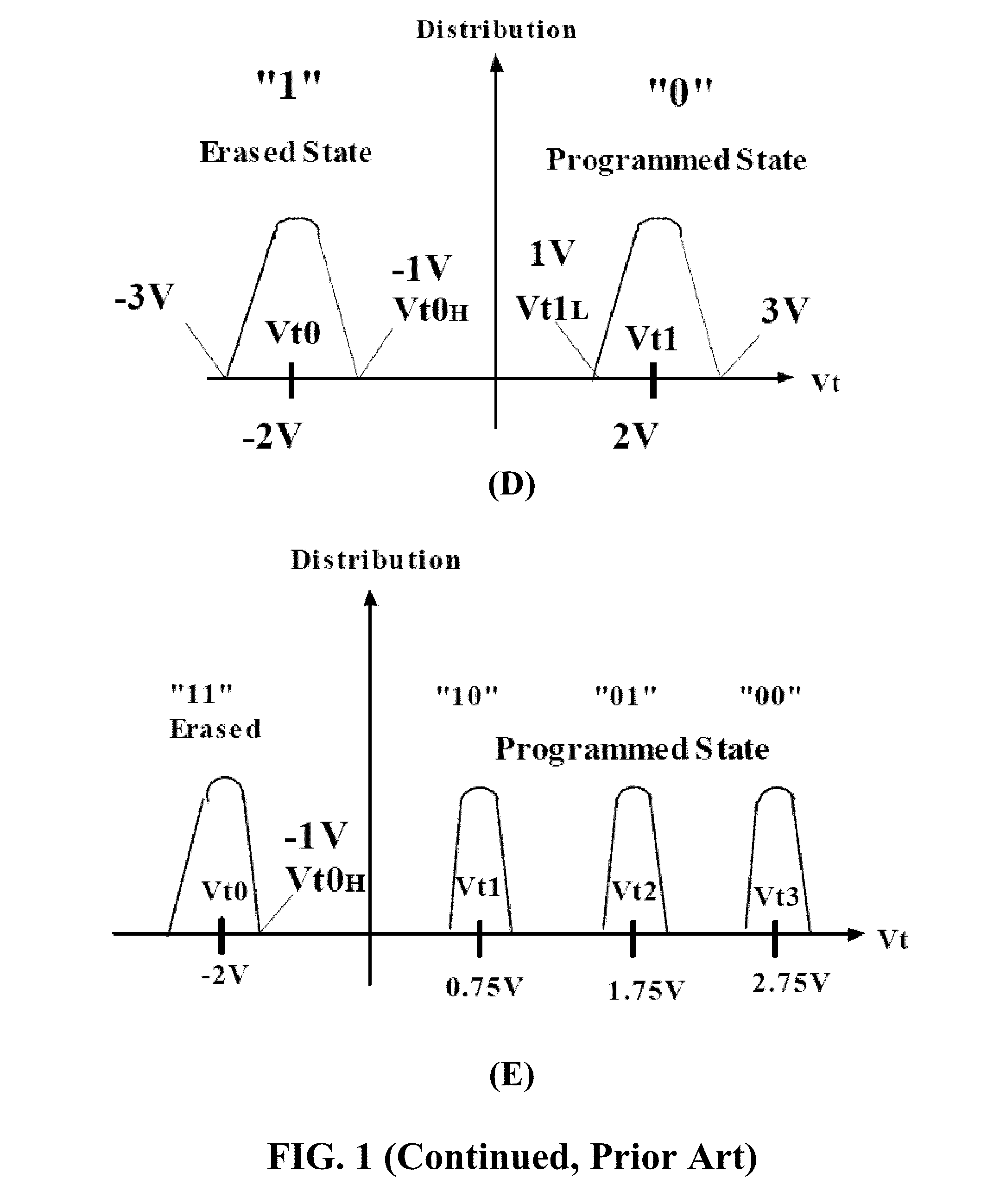
[0068]Conventional NAND flash memories use Fowler-Nordheim (FN) tunneling scheme to perform block erase and page program operations. ETOX™-based NOR flash memories use FN to perform block erase operations and use channel hot electron (CHE) to perform program operations in unit of byte or word. Due to the inherent over-erase concern and the nature of high-power consumption of the CHE operation of ETOX™-based NOR flash memories, the program speed of the conventional NOR flash memory is 50 times slower than the NAND counterpart in page program operations. Similarly, the erase speed of the NOR flash memory is 500 times slower than that ...
PUM
 Abstract
Description
Claims
Application Information